Sine wave driver determines system noise.
Dr. William O’Brien, Mad City Labs Inc.
Nanopositioning is a basic requirement in virtually all areas of nanotechnology research. And, because it implies very small motions controlled with a high degree of accuracy, it seems intuitive to seek a specification of a nanopositioner’s resolution; that is, what is the smallest motion producible by a given design? Some applications, such as those involving optical microscopy, often do not test the limits of a nanopositioning device. Others, such as laser particle tracking, may push the limits of nanopositioning resolution.
Nanopositioners use ceramic piezoelectric actuators made of lead zirconate titanate (PZT) to create the driving force within the mechanical positioner. An actuator responds to an applied voltage by changing its length. Because an actuator is an analog device, the smaller the voltage applied, the smaller the change in length. An infinitely small signal with zero noise would produce a correspondingly small change. Inside the nanopositioner, the actuator is tightly constrained and preloaded to eliminate unwanted mechanical play in the system. In other words, there is no limiting resolution fundamental to the nanopositioner design.
An additional complication is that a highly accurate nanopositioner incorporates one or more position sensors that provide a feedback signal to the system’s electronic controller. Each sensor enables the controller to continuously adjust the driving voltage to maintain the positioner at a fixed point. Therefore, the term “resolution” is best thought of as the smallest signal that can be accurately passed through the controller and applied to the actuator in combination with the smallest motion detected by the sensors and fed back to the controller.
Because any electronic system has an intrinsic level of noise — however low — that imposes the fundamental limit on small signals, the resolution specification refers to the noise expressed in terms of physical motion. To more accurately define resolution as it relates to nanopositioning, the term “position noise” was coined to reflect the effect of noise on the complete system. Accurate motions cannot be produced or measured at dimensions below the specified position noise.
Measuring the position noise on nanopositioner designs is difficult. Low-noise amplifiers, combined with low-impedance, low-noise sensors, produce a position noise that is well below the limits of precision instrumentation. In the subnanometer range, even interferometry cannot take measurements with the required accuracy.

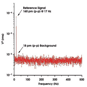
Figure 1. A power spectrum of a position sensor signal shows a 17-Hz sine wave and background noise.
A technique developed by Mad City Labs Inc., however, provides a direct method of accurately determining position noise by driving a nanopositioning system with a sine wave signal scaled to produce subnanometer peak-to-peak motion while continually digitizing and analyzing the output signal from the position sensor. A fast Fourier transform of the sensor signal will show a spike at the driving signal’s frequency. Using the transform power spectrum to scale the level of background noise, the system’s position noise routinely is shown to be <0.1 nm.
Based on these calculations, the minimum resolvable motion of the company’s 100-μm-range nanopositioning system is 0.1 nm, which represents a position noise of one part in 1 million. Although this resolution may be well below the capability of the user’s input signal circuitry, it does illustrate the limitation of the nanopositioner with its associated controller.
If a digital-to-analog converter is used to provide the input positioning signal, 20-bit resolution is needed to produce a range of input signals equivalent to the complete resolution of the nanopositioning system. A more typical converter with 16-bit resolution would provide only one-sixteenth of the nanopositioner’s available resolution.
Meet the author
William O’Brien is a member of the R&D group at Mad City Labs Inc. in Madison, Wis.; e-mail: [email protected].