YORKTOWN HEIGHTS, N.Y., Nov. 3 -- IBM today announced its researchers have used photonic crystal technology to "slow light," a process that could lead to the use of light instead of electricity in the connection of electronic components and optical communications circuits, which scientists say could make those components work vastly better.
Scientists have searched for practical ways to use light to speed communication between the components within a computer. But, to be realistic, the components to support such an optical network need to provide excellent control over the light signal while also being very small and inexpensive to manufacture. IBM researchers say their work addresses several pieces of this puzzle.

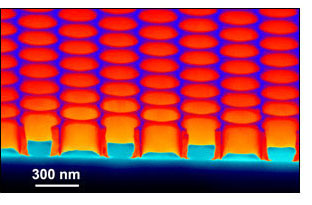
A false-colored scanning electron microscope image of a photonic crystal composed of a periodic array of holes etched in a silicon slab. (Photo: IBM)
The IBM team was able to slow light down to less than 1/300th of its usual speed by using a photonic crystal waveguide -- a thin slab of silicon punctuated by regular arrays of holes that scatter light. The pattern and size of the holes gives the material a very high refractive index -- the higher the refractive index, the slower the light. Heating the waveguide locally with a small electrical current alters the refractive index, allowing the speed of light to be quickly tuned over a large range with very low applied electric power.
Researchers have known for some years how to slow light to a crawl under laboratory conditions, but actively controlling the light speed on a silicon chip, using standard silicon with standard micro- and nanoelectronic fabrication technology, is a first, according to IBM. The device's small size, the use of standard semiconductor materials and the ability to more closely control this "slow light" could make the technology useful for building ultracompact optical communications circuits that are practical for integration into computer systems, researchers say.

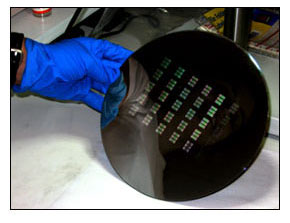
A silicon-on-insulator (SOI) 200-mm wafer processed on a standard CMOS fabrication line with numerous nanophotonic circuits. (IBM photo)
The active area of the IBM device is microscopically small, indicating the possibility of complex light-based circuits with footprints not much larger than semiconductor circuits. The manufacturing processes used to build the device are available in nearly any semiconductor factory. Researchers say the capabilities demonstrated could be applied to create a variety of nanophotonic components such as optical delay lines, optical buffers and even optical memory, all of which would be useful in building computer systems knitted together by powerful optical communications networks.
The report on this research, "Active Control of Slow Light on a Chip with Photonic Crystal Waveguides" by Yurii A. Vlasov, Martin O'Boyle, Hendrik F. Hamann and Sharee J. McNab of IBM's T.J.Watson Research Center in Yorktown Heights, is published in the Nov. 3 issue of the journal Nature. This work was partially supported by the Defense Advanced Research Agency (DARPA) through the Defense Sciences Office program "slowing, storing and processing light."
For more information, visit: www.research.ibm.com