New sensor technology is ideal for inspecting flat panel displays, wafers, printed circuit boards and document scanning.
JUNGHYUN NAM AND WOJCIECH MAJEWSKI, VIEWORKS CO. LTD.
Time delay integration (TDI) sensors have been around for almost 40 years now. The concept originated from the days of film cameras, when the idea of opening the shutter and rolling the film at the same speed as the moving target recorded a seemingly static image on the film.
With the introduction of CCD imaging technology in the 1970s, the concept was applied to designing the first TDI sensors only a few years later. The sensor structure consists of line scan sensors with a large number of pixels (the largest sensor today has 23k pixels), which are added in parallel. The resulting sensor resolution is equal to the number of pixels in one line multiplied by the number of lines, also called stages. It works by recording an image several times by each sensor line, and the recording is added onto the next recording line until the final line is reached. The end result is an image accumulated from all the lines, resulting in the increase of sensitivity equal to the number of lines. A TDI sensor with 256 lines, for example, should allow a 256× increase in sensitivity. Of course, this is a simplified view; the reality is a bit more complex and the realized sensitivity increase somewhat lower. All existing TDI sensors until now have either used CCD or CMOS technology — and both have their inherent advantages and disadvantages.
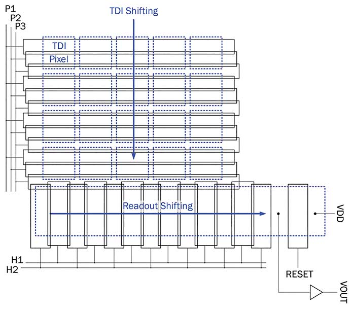
Figure 1. Structure of a CCD time delay integration (TDI) sensor. Courtesy of Vieworks Co. Ltd.
CMOS vs. CCD
CCD TDI sensors (Figure 1) have been around for many years and their main advantage was the simple fact that only the electrical charge was being moved during the integration process. Practically no noise increase happens during the charge accumulation process. This, in combination with the use of CCD photosites on the sensor, results in a high dynamic range and generally lower levels of noise, which are typical for CCD technology. The only exception is the dark noise, which is usually higher in CCD TDI sensors due to very high line sampling frequency. Dark noise, derived from dark current, is thermally generated electrons moving around in the photosites even with no light hitting the device.
The main disadvantage of the CCD TDI sensor is analogue output, which requires adding extra circuitry outside of the sensor such as A/D converters, horizontal and vertical drivers, and CCD amplifiers. These enhancements add extra complexity and cost at the system level as well as additional heat, causing higher noise. They also add excessive power consumption.
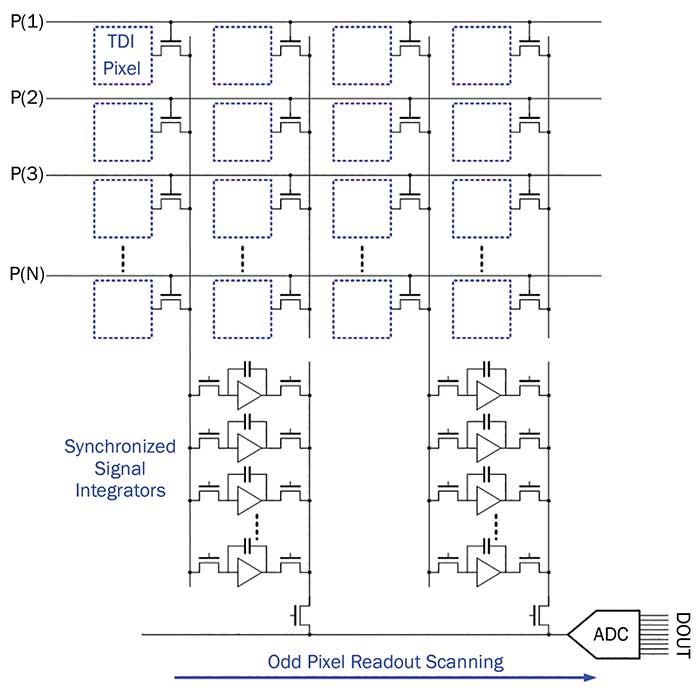
Figure 2. Sample structure of a CMOS TDI sensor. Courtesy of Vieworks Co. Ltd.
The introduction of CMOS TDI sensors (Figure 2) eliminated most of the problems related to analogue signal output in CCDs. The use of internal analogue-to-digital converters (ADCs) allows for digital output and increases the speed of data rate. The power consumption is much lower than that of CCD TDI sensors. Accumulating the signal electronically increases the sensitivity, but at the same time increases the noise in the signal by repeating the conversion process.
Several groups have worked on eliminating the deficiencies of the two technologies. There have been some positive developments in recent years, notably by Imec, which in 2013 demonstrated samples of the hybrid TDI sensors called CCD in CMOS. Unfortunately, this technology hasn’t been commercialized and remains in a prototype stage.
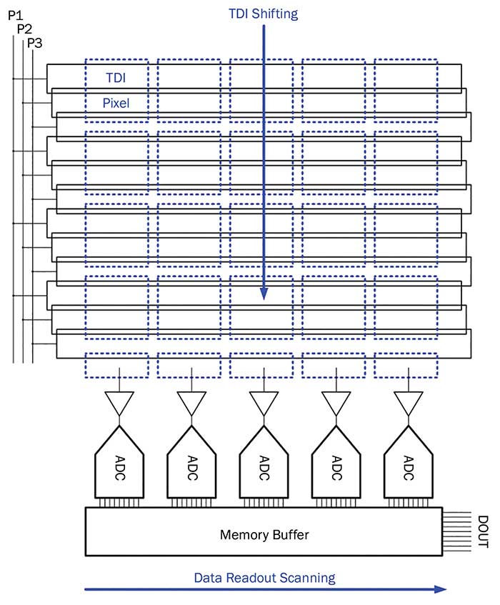
Figure 3. Basic structure of a hybrid TDI sensor. Courtesy of Vieworks Co. Ltd.
In 2016, after several years of development, the first commercial hybrid sensor debuted, combining the best features from both CCD and CMOS sensors and leaving out most of the undesirable properties (Figure 3).
Hybrid sensor: Best of both worlds
The hybrid sensor design incorporates a CCD pixel array with over 90 percent fill factor. Use of CCD photosites ensures a high image quality in terms of signal-to-noise ratio and virtually noiseless charge transfer in the CMOS TDI where noise increases in the signal during the accumulation process. The CMOS structure of the chip with built-in ADCs permits high readout speed and digital output, eliminating the need for costly and complex external circuitry. In addition, power consumption is only 25 percent that of comparable CCD TDI sensors.
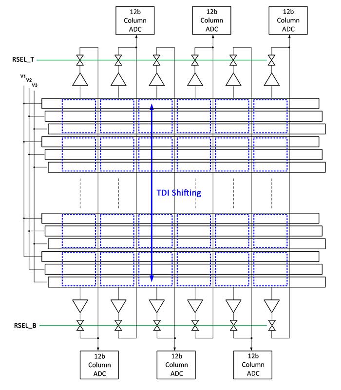
Figure 4. Advanced structure of a hybrid TDI sensor. Courtesy of Vieworks Co. Ltd.
In order to develop the hybrid sensor, several steps were added to the CMOS fabrication process in order to implement CCD photosites embedded within the CMOS circuits. One of the biggest challenges was that CMOS device parameters could not be affected, so only limited process changes were possible. To overcome this, engineers worked closely with a semiconductor fabrication foundry to implement TDI-optimized CCDs, with a charge transfer efficiency of 99.99 percent or more, based on a 110-nm CMOS base line process.
The next critical challenge was implementing analogue circuits such as correlated double sampling and an ADC for each CCD output (Figure 4). Since the CCD has a limitation on the charge transferring speed, it is advantageous to use a CMOS method in which each signal is processed in parallel, rather than serialized, as it is done on existing CCD-type TDI sensors. Another method is to share an ADC through an analogue multiplexer by bundling several columns to implement a signal processing circuit with a narrow pixel pitch.
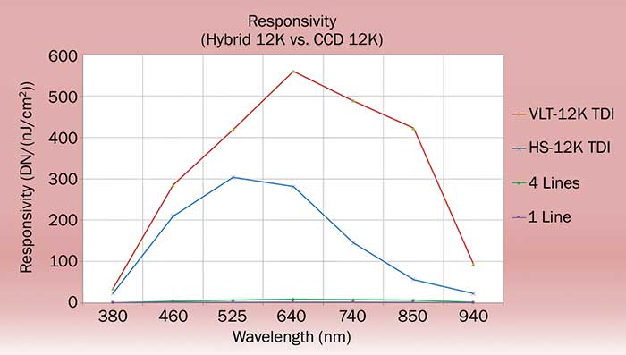
Figure 5. Responsivity comparison among hybrid TDI, CCD TDI, CMOS 4-line and line scan cameras. Courtesy of Vieworks Co. Ltd.
However, this method poses a problem in that the signal-to-noise ratio and the power consumption increase. In addition, a fixed pattern noise is likely to occur due to characteristic differences between ADCs. In the hybrid TDI, correlated double sampling and ADC are designed for each column, which operates at low power consumption and achieves high uniformity. This method is the most popular in CMOS image sensors.
In order to realize a 12-bit high-performance ADC with a narrow column width, a method of crossing the odd-column and even-column circuits to the upper and lower portions of the imaging area is also possible in a CMOS circuit. To accomplish this, a signal line is placed between the pixels, so that the amplified output signal from the source follower amplifier connected from the CCD output stage can be freely connected to the upper or lower signal processing circuit. For bidirectional TDI operation, CCD output stage must be installed at both sides and the top and bottom. By selectively connecting each output signal to the signal line installed between the pixels through the selector, the bidirectional TDI corresponding configurations are possible. In this way, hybrid TDI sensors can go down to 3.5-μm pixel pitch.
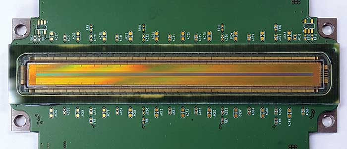
Figure 6. 23k × 256 TDI sensor from Vieworks. Courtesy of Vieworks Co. Ltd.
In a typical semiconductor process, the maximum length of the chip size does not exceed 32 mm. To create a sensor with a size larger than this limit, a method called stitching is used. The image sensor such as TDI repeats the same pattern in the center sensor area. Therefore, it is possible to fabricate semiconductors by duplicating the central pattern by repeating the manufacturing process of the left and right, driving circuit portions and the central repeating pattern in a separate region on one photo mask. However, this method has been known to be possible only in the 180-nm class, because the continuity and uniformity of the pattern-connecting portion is guaranteed by the actual fabrication process environment. Vieworks Co. Ltd. worked with FabFoundry to set up a stitching process in a 110-nm process and succeeded in securing a stable quality level. In this way, it is possible to manufacture sensors of various sizes according to the working method with the same photo mask set. This allows the manufacture of TDI image sensors with a maximum imaging depth of 164 mm and 3.5-μm pixel pitch on a 200-mm wafer.
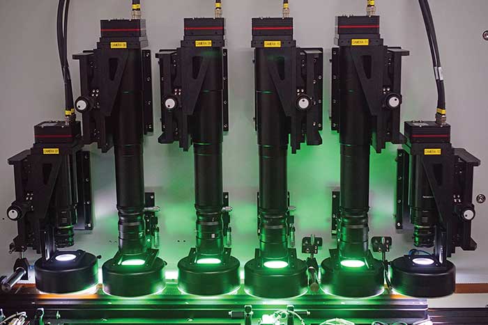
Figure 7. Inspection system using 18k TDI cameras. Courtesy of Warpvision Inc.
Hybrid TDI technology fares well in comparison to others (Figure 5). The tests of responsivity at the same system gain (e−/DN) and bit depth have shown the responsivity to be almost twice that of a comparable CCD TDI camera. Two 12k × 256 cameras have been tested in compliance with the EMVA1288 Standard. The values for maximum signal-to-noise ratio were 46 dB (200:1) for hybrid TDI camera vs. 44 dB (160:1) for CCD TDI camera; the dynamic range was 66 dB (2000:1) vs. 57 dB (750: 1); and the dark noise level at the maximum gain was 14 e− vs. 33 e−, respectively.
Since the introduction of the technology, a number of TDI cameras have been developed, starting from horizontal resolution of 3k with 32 stages on a pitch of 7 μm to 23k with 256 stages on 3.5-μm pixels with line speeds of up to 250 kHz (Figure 6). These new and innovative products have already been adopted by customers requiring high-speed and light-sensitive applications and are gaining even more popularity.
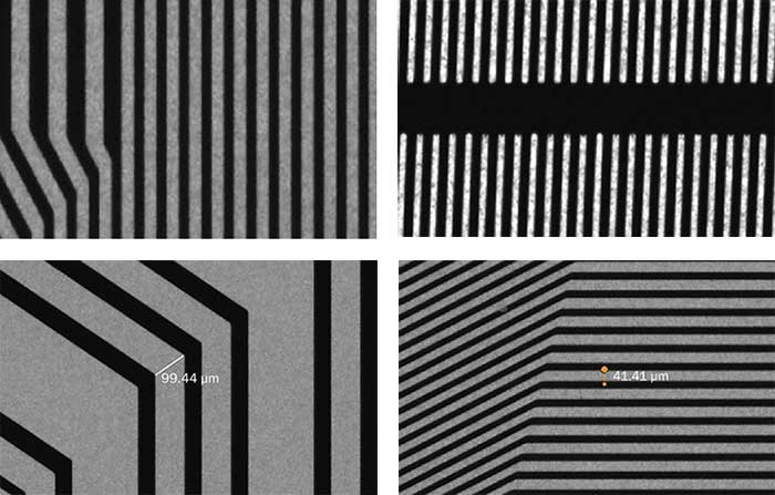
Figure 8. Image of chip-on-film taken with a TDI camera. Courtesy of Warpvision Inc.
An interesting example of using hybrid TDI cameras is automated optical inspection for chip-on-film packages — an application that calls for a line scan camera with lower noise, a higher dynamic range and fine pixel pitch. Developed by Warpvision Inc. from Suwon, Korea, the system (Figure 7) uses 18k TDI cameras with 3.5-μm pixel size and 256 stages. The special pixel pitch or resolving power is 1 μm using 3.5× magnification. The system has dual purpose: It inspects the circuits as well as the surface (Figure 8). Ultimately, automated optical inspection in electronic production needs a higher resolution to inspect the fine pitch circuits as chip-on-film technology develops.
The innovative and potentially disruptive hybrid TDI technology could find additional uses in flat panel displays, printed circuit boards and document scanning.
Meet the authors
Junghyun Nam, Ph.D., is the chief designer at Vieworks Co. Ltd.; email: [email protected]. Wojciech Majewski is Vieworks Co. Ltd.’s sales director; email: [email protected].