The optimization of multijunction VCSEL architectures offers an immediate benefit to automotive lidar and other high-power sensing applications.
AMIRHOSSEIN GHODS AND KLEIN JOHNSON, OSRAM
Vertical-cavity surface-emitting lasers (VCSELs) have garnered significant attention for various
sensing and visualization
applications during the past three decades. The sustained progress in their development during this period owes largely to advanced semiconductor growth technology, as well
as enhanced expertise in device fabrication processing. Specifically, VCSELs emitting in the near-infrared spectrum, ~800 to 1200 nm, and using the gallium arsenide/aluminum gallium arsenide (GaAs/AlGaAs) material system, have consistently improved in terms of their performance and range of supported
applications.

Manufacturers favor the use of vertical-cavity surface-emitting lasers (VCSELs) for their compact size and efficiency. While they have been used in a variety of products and systems during the past 30 years, a preeminent implementation is in automotive lidar to more effectively sense the environment around a vehicle. Courtesy of iStock.com/ArtemisDiane.
Short-distance data communication and spectroscopy and biosensing — which require low-to-moderate optical output power(s) — are common applications for VCSELs. These lasers are favored for their compact size and high efficiency. Further, manufacturers can design and develop VCSELs in large arrays.
Such a design makes VCSELs suitable for integration into a wide variety of devices and systems. The introduction of 3D sensing with the iPhone “Face ID” feature in 2017, for example, significantly boosted the use of VCSELs in various consumer electronics, augmented reality/virtual reality devices, drones, automotive in-cabin monitoring and gesture recognition systems, and payment systems. This advancement, targeting the consumer, spurred innovation in system and product development; new applications emerged and existing applications improved and evolved.
More than half a decade later, VCSEL technology is expanding again and
penetrating fields such as industrial
automation, medical diagnostics, and
environmental monitoring. A core application area for the present wave of VCSEL technology is high-power
sensing, which envelops distance lidar applications, such as automotive for advanced driver-assistance systems (ADAS) and self-driving vehicles. Automotive lidar manufacturers use different architectures to create a 3D map of the environment in front of, and sometimes around, the vehicle, actively scanning the surrounding areas. These systems are essential to improve safety and enable autonomous navigation.
To date, edge-emitting lasers (EELs) have dominated regarding the types of laser systems in the lidar market. Systems designers and integrators often select these lasers since they can achieve high output optical power levels.
Recent advancements in the development of high-power multijunction
VCSELs capable of producing output power densities well above 1 kW/mm2 are now positioning VCSELs as a desired substitute. These high-power multijunction sources are a cheaper and more efficient replacement for traditional EELs. Additionally, VCSELs demonstrate better temperature performance than their EEL counterparts, as well as narrower spectral width(s), and a circular beam shape that benefits certain applications, including high-power automotive lidar.
Prefabrication optimizations
Several parameters influencing performance distinguish VCSELs developed for lidar applications from early iteration
VCSEL technology as well as from EELs and other laser systems. First, these devices are designed to emit between 900 and 940 nm. This wavelength range minimizes the effect of the background ambient solar spectrum and enables a higher signal-to-noise ratio and detection efficiency. Moreover, silicon (Si) photodetectors, which are typically used in automotive and industrial lidar modules, exhibit peak responsivities around this wavelength range.
Second, the output optical power, especially for long-range lidar >300 m is typically desired to be >1.5 kW/mm2. Also, a narrow beam divergence angle <25° could help deliver the optical power to a further distance and increase the object detection efficiency of the lidar module.
Increasing the number of active light-emitting junctions is an effective approach to scale the output power — and external quantum efficiency — of VCSELs. In this method, several pin junctions are series-connected, and tunnel junctions, placed in between the active junctions, provide the electrical and
optical coupling between the junctions. These tunnel junctions are made of ultrathin layers of highly p- and n-doped semiconductor materials, which facilitates the process of charge carrier recycling
between the neighboring active junctions1. In other words, electron-hole pairs injected into bipolar cascade active regions recombine in an active multiple-quantum-wells (MQWs) region and are subsequently regenerated in the adjacent tunnel junction.
In this way, the pairs recombine in the neighboring MQWs stage as well. This process can multiply, as to the number of active MQWs stages, which leads to the possibility of scaling output power while maintaining injected current levels.
Increasing the gain volume in a multijunction VCSEL also makes it possible to reduce the effective reflectivity of the system mirrors without changing the lasing threshold gain. This in turn enables the extraction of more light without
increasing the threshold current and lowers the series resistance and voltage, and
it increases the power conversion efficiency (PCE) of these devices.
Alternatively, a more complex cavity structure in multijunction VCSELs complicates the design process and overall laser design and may adversely influence electro-optical performance. For example, increasing the number of active junctions can cause a significant increase in the far-field beam divergence2. The number of oxide layers in a multijunction structure is likely responsible for this increase, and it also increases the refractive index contrast between the core and the cladding regions of the VCSEL. This may lead to the wider beam divergence angle. The nonuniformity of the oxide fronts in a multijunction VCSEL can further lead to an increase of the “oxide-modes,” which is exemplified as higher-order transverse modes in the 2D far-field beam profile or as additional side-peaks in the emission spectrum.
The use of mode filters can suppress the stimulation of these higher-order transverse modes and narrow the divergence angle in multijunction VCSELs. These filters, typically etched at the emitting surface of the device, increase the mirror losses for the higher-order transverse modes, which are emitted at wider angles. At the same time, they ensure that the lasing threshold gain for the transverse modes emitting at narrower angles is unchanged.
Device fabrication and characterization
Especially for use in high-power lidar devices, the characteristic performance of the power sources is a core consideration for the detection mechanism. In recent R&D efforts, ams OSRAM fabricated eight-junction (8J) VCSEL dies, both in the form of a single-aperture die and a densely packed array die. Results from tests performed under varying conditions showed that the multijunction VCSELs produced output power densities
>2 kW/mm2 with desirable slope and power conversion efficiencies. Both values are favorable in common EEL performance for use in high-power automotive lidar devices.
The multijunction structure of the
fabricated devices consisted of eight active light-emitting PIN junctions, in which each junction enclosed MQWs for emission at 905 nm. The epitaxial structure of the 8J VCSEL was grown using metal-organic chemical vapor deposition
on an n-type GaAs substrate. Two distributed Bragg reflector (DBR) mirrors were positioned to surround the active regions. The mirror pairs for both top and bottom mirrors achieved reflectivities >99%. The reflectivity of the top p-DBR mirror was slightly lower than the bottom n-DBR mirror, allowing the device to be top-emitting.
Figure 1 shows highly-doped p+/n+ tunnel junctions providing electrical
coupling between the active junctions.
An ultrathin, high-aluminum content
AlGaAs oxide layer was placed above each active junction to provide lateral electrical and optical confinement. The tunnel junctions and the oxide layers were positioned at the null of the standing
electrical field inside the cavity to minimize the internal losses. The MWQs’ active stages are placed at the peak of
the field to maximize modal gain.
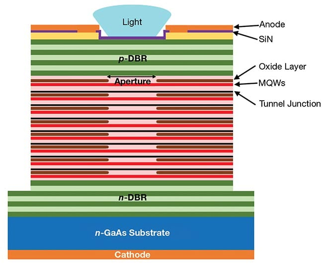
Figure 1. A cross section of the eight-junction (8J) VCSEL epitaxial structure. The epitaxial design of multijunction VCSELs enables output power scaling while maintaining die footprint. High-power sensing applications, including automotive lidar, require a high output optical power density. DBR: distributed Bragg reflector; GaAs: gallium arsenide; MQWs: multiple-quantum-wells; SiN: silicon nitride. Courtesy of ams OSRAM.
ams OSRAM used UV lithography to fabricate the VCSELs and dry etching and wet oxidation to form circular mesas and the oxide apertures, respectively. Silicon nitride was used as the passivating material for the etched sidewall areas and the antireflective coating layer at the top surface, and top p-type and bottom
n-type ohmic contacts were deposited. The dies were then singulated and packaged onto ceramic substrates for characterization.
The researchers characterized the performance of the VCSEL dies by measuring their power-current-voltage (L-I-V) properties under continuous wave (CW) conditions for single-aperture die, and short-pulse conditions for the VCSEL array die. The researchers also charted spectral response and far-field beam profiles.
Interpreting results
Figure 2 shows the L-I-V characteristics of single-aperture 8J VCSEL dies with varying oxide aperture sizes, between 6 and 20 µm, measured at room temperature. For this design, increasing the aperture size resulted in increases in both the lasing threshold current and available output power. The total voltage mainly consisted of the voltage drop across the eight active junctions, ~1.4 V/junction, in addition to the voltage across each tunnel junction, ~0.1 V/tunnel junction. Figure 2 also reflects the drop caused by the DBR mirrors.
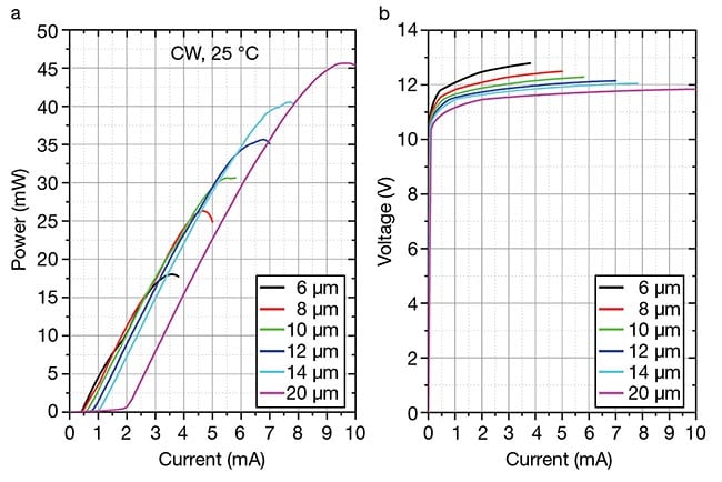
Figure 2. The power-current (L-I) characteristics of the single-aperture 905-nm eight-junction (8J) VCSEL die, with varying oxide aperture size, as measured at room temperature (a). The corresponding current-voltage (I-V) characteristics (b) show correlation to an increased lasing threshold current and available output power. CW: continuous wave. Courtesy of ams OSRAM.
Each of the fabricated VCSEL devices achieved a PCE of >40% and slope efficiency of >7 W/A. Due to a rise in junction temperatures under CW testing conditions, all devices exhibited a thermal rollover at higher injected bias current levels.
Figure 3 shows the far-field beam
profiles of the 20-µm aperture VCSEL die at two bias currents as well as the 1D cross section of the far-field beam profiles. Both beam profiles are highly multimode, with several higher-order transverse modes lasing simultaneously, forming a doughnut-shaped beam.
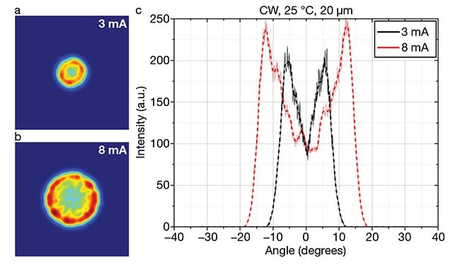
Figure 3. Far-field beam characteristics of the 20-µm single-aperture VCSEL die are measured at 3 mA (a) and 8 mA (b). The cross-section beam profiles (c) show an increase in the beam divergence angle, as initiated by increasing bias current: The beam increases by increasing the bias current level from ~15°, which is caused by the increase in the number of higher-order transverse modes that typically emit at wider angles. Courtesy of ams OSRAM.
Predicting performance
In subsequent fabrication, ams OSRAM developed a VCSEL die, in the form of
a linear array of apertures, which included more than 50 apertures, where each oxide aperture has a diameter of 20 µm. The apertures were hexagonally packed in an emission area of 1500 × 60 µm. The fabricators measured the electro-optical characteristics of this VCSEL die under short-pulse test conditions, with a pulse width of 10 ns and duty-cycle of 0.1%. Figure 4 shows both the injected current signal as well as the output light pulse.
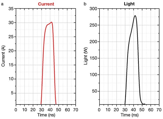
Figure 4. A VCSEL die in the form of a linear array of >50 apertures (below). The electro-optical characteristics of this die were measured under short-pulse test conditions. The bias current signal is pulsed into the VCSEL with a peak of ~30 A (a), and the output light pulse is charted (b). Courtesy of ams OSRAM.
The L-I characteristics of the VCSEL array die measured under short-pulse test conditions is shown in Figure 5a. A peak power as high as ~330 W at the pulsed current of ~40 A, and corresponding to power density of ~4 kW/mm2 at the current density of ~200 kA/cm2 was achieved. However, for reliable operation of VCSELs, the bias pulsed current is typically limited to <100 kA/cm2,
where a peak output optical power of
175 W, corresponding to a power density of 2.1 kW/cm2, is achieved. Figure 5b shows the calculated power conversion
efficiency at different current levels, where the PCE reached ~27% at the
current density of 100 kA/cm2. The peak PCE for this device was measured at ~48% at 4 A, corresponding to a current density of ~20 kA/cm2. The average slope efficiency was ~8.5 W/A.
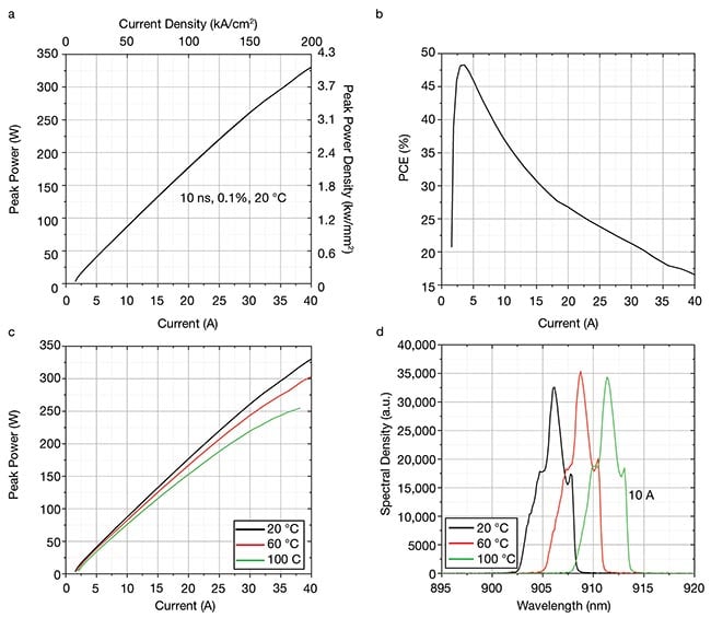
Figure 5. Power-current (L-I) characteristics of the eight-junction (8J) 905-nm VCSEL array die, measured at 20 °C, are charted (a), as well as the calculated power conversion efficiency (b). The L-I characteristics are shown at different substrate temperatures (c); for example, at ~20 A (i.e., 100 kA/cm2), the total measured output power is ~175 W, whereas it decreases by ~15% (to ~150 W) at the substrate temperature of 100 °C. The temperature-dependent spectral response of the VCSEL array die is additionally shown (d). PCE: power conversion efficiency. Courtesy of ams OSRAM.
Figure 5c shows the temperature-dependent L-I characteristics of the VCSEL array die: The total output power decreases by increasing the substrate
temperature. Similarly, the temperature-dependent spectral response of the VCSEL array die shows that the device emits at ~905 nm at 20 °C, and subsequently, red-shifts to longer wavelengths by increasing substrate temperature
(Figure 5d). The red shift is mainly caused by the shift in the cavity resonance wavelength, in addition to the shift in the bandgap energy of the active gain material. The side-peaks in the emission spectra demonstrate that the fabricate devices are highly multimode.
Figure 6, showing the far-field beam characteristics of the VCSEL array die, details the 2D beam profiles of the VCSEL at the bias current of ~10 A and two different substrate temperatures (Figure 6a,b). A circular flat-top beam profile can be observed under both test conditions, despite the observation of the VCSEL die under CW test conditions where a doughnut-shaped far-field beam pattern is typically observed. Under CW test conditions, the effect of thermal lensing, which is caused by the rise in the junction temperature, could lead to the stimulation of additional higher-order transverse modes that typically emit at wider angles. On the other hand, in the short-pulse test regime, the lack of such a mechanism could contribute to a more evenly distributed beam profile.
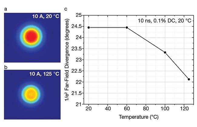
Figure 6. Far-field beam characteristics/profiles (a-b) of the eight-junction (8J) 905-nm VCSEL array die. The calculated 1/e2 beam divergence angle is shown against substrate temperature (c), where the divergence angle drops from ~24.5° at ~20 °C to ~22.1° at ~125 °C. This reduction in divergence angle could be partly caused by improved lateral current, which is spreading across the oxide aperture at higher temperatures. Overall, the divergence angle is within the range to support automotive lidar applications, in which divergence angles <25° are desired. DC: duty cycle.
Courtesy of ams OSRAM.
Meet the authors
Amirhossein Ghods is a senior staff scientist at ams OSRAM. He leads the EPI design activities for NIR III-V surface-emitting lasers targeted for a variety of 3D-sensing and
automotive lidar applications; email: amir
[email protected].
Klein Johnson has been working in the field of VCSEL technology since the early 1990s, first with Honeywell and later as cofounder
of Vixar. He currently leads VCSEL R&D
activities at ams OSRAM; email: [email protected].
References
1. T. Knodl et al. (2003). Multistage bipolar cascade vertical-cavity surface-emitting lasers: theory and experiment. IEEE J
Sel Top Quantum Electron, Vol. 9, No. 5,
pp. 1406-1414.
2. A. Ghods et al. (March 2024). High-Power Multijunction VCSELs for LiDAR and Related Sensing Applications. Proc SPIE Light-Emitting Devices, Materials, and
Applications XXVIII, Vol. 12906, Article No. 88, San Francisco, Calif.