Hank Hogan, Contributing Editor
Advances in computer technology have made software applications in
the photonics industry commonplace, enabling users to transcend the limitations
of their hardware.
Increasingly inexpensive computing solutions are enabling users to
reconfigure their instruments and to manipulate data as never before, overcoming
the constraints of hardware to optimize photonic applications. When a photonics
problem is too difficult for the hardware to handle, the intelligent use of software
can offer a solution.
For example, if the pixel density is too low for
an imaging application, using software to pull information out of the dark may be
the best answer. And if eliminating distortion optically is too costly or even impossible,
researchers and industrial users may find that software processing is a better approach.
In another example, semiconductor manufacturers
may employ software-controlled distortion to print subwavelength-size patterns reliably.
Conceptually, it’s the reverse of using software to clean up an image. Numerical
Technologies Inc. of San Jose, Calif., is counting on this process becoming the
standard and ushering in a fundamental change in semiconductor photolithography.
“You are moving away from the
‘what you see is what you get’ to a very convoluted, nonlinear set of
relationships that really has no other way of being controlled other than through
software,” said J. Tracy Weed, senior director of marketing and business development
for the company.
But there are limitations. Broadly
speaking, the old adage “garbage in, garbage out” still applies.
“The biggest limitations in the
end are how accurately the optical distortion can be specified — which greatly
affects the quality of the reconstruction — and how much distortion you can
correct before degrading the image so much that it no longer meets your needs,”
said Chris Cox, a senior computer scientist with Adobe Systems Inc. of San Jose.
A warped view
Adobe’s popular Photoshop is the commercial
image-editing standard, and it has spawned a host of applications. Many fall into
a category alternatively known as image warping, geometric image correction or image
resampling. These terms mean the same thing: the stretching of an image to create
a desired effect or correction.
Paul Heckbert, on leave from his position
as an assistant professor in the computer science department at Carnegie Mellon
University in Pittsburgh, is working as a 3-D graphics architect at Nvidia Corp.
in Santa Clara, Calif. He explained that “image warping” is popular
in the computer graphics arena and “geometric image correction” in remote
sensing, and that one is prone to encounter “image resampling” in image
and signal processing.
He said that the process, whatever
the name given it, is well-understood and presents few disadvantages. “I can’t
think of any, unless you do a poor job of it,” he said.
One pitfall, however, is improper antialiasing,
or smoothing the jagged appearance of lines. In antialiasing, the software adjusts
the position and intensity of pixels at the edge of a figure, such as the boundary
of a black letter on a white background. If this is done incorrectly, the adjusted
data can lead to false images and other artifacts.
The idea behind these software operations
is that applying a mathematical transformation changes the relationship between
pixels, resulting in the selective stretching of an image. In entertainment applications,
for example, they alter the features of characters and their surroundings and enable
animals to spout words of wisdom.
In research and industry, such software
may remove distortions and flatten, or dewarp, images. Distortion may be due to
imperfections in the lens system, and software may be the most cost-effective way
to remove it. “It is a lot easier to correct for small optical distortions
in software than it is to construct and align a perfect optical system,” Cox
said.
One example is the distortion found
in pictures taken through a zoom lens. The image can pincushion, in which case the
center bows in or bulges outward. A photographer may use tools based on Photoshop
to remove these distortions and straighten the image.
Similar problems and comparable solutions
appear in industrial applications that use cameras and lenses. A microscopic examination,
for instance, may employ geometric image correction to remove lens aberrations and
magnification differences from the center of a field of view to the edge.
Out of the dark
But there are other cases where the problem lies
not in the lens, but in the data. Octavo, a small company in Oakland, Calif., creates
digital versions of old manuscripts, books and other media for sale on CD-ROM and
in downloadable format. Such media may be very fragile and sometimes cannot be opened
fully without suffering damage. Octavo opens the volumes as much as is safely possible
and images the text under very high resolution.
The company’s scanning system
uses a 10,500 x 12,600-pixel digital array, a wide-body camera and specialized lighting
to achieve extremely high quality results. Once the data is captured, software digitally
dewarps the image. The result is an artificially flattened electronic version that
looks like the original would if it could be opened.
If dewarping is not enough, other software
techniques may be used. One problem that frequently is encountered is not a hardware
limitation, but a fiscal constraint. A research program, for example, may have a
limited budget, and the optimal hardware solution, such as an advanced digital camera,
may be too expensive. The most cost-effective solution may be a less-expensive,
lower-resolution camera combined with software.
Bloomy Controls Inc. of Windsor, Conn.,
is a systems integrator and consulting company for a variety of industrial and research
customers. The company may be called upon to pull data out of “thin pixels”
— that is, to engineer an inexpensive camera and lens approach that reproduces
the resolution of more costly hardware. In such cases, principal engineer Robert
Hamburger may suggest software to sprinkle new data between the existing pixels.
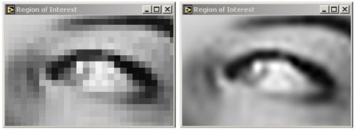
One application of software in photonics
is to enhance the performance of hardware to approximate that of more advanced systems.
The image on the left is a low-resolution close-up of a woman’s eye. On the
right, a cubic spline interpolation yields a 10x enhancement in the image, revealing
a glint in the eye as well as blood vessels in the sclera. Courtesy of Bloomy Controls
Inc.
This interpolation works, but its limitations
must be taken into account. “Pixel interpolation has greater confidence and
higher validity away from the edges of the image so that any particular place where
you’re trying to make an accurate measurement, you have enough data in enough
directions so that you’re not close to the boundaries of the interpolation,”
he said. “That’s one of the caveats.”
 Bloomy Controls is a close partner
of National Instruments Corp. in Austin, Texas, and uses its products. Hamburger
often employs the company’s array of image manipulation software tools. He
said that the power of these software packages and the easy implementation of the
tools enable him to concentrate on systems integration rather than on writing low-level
processing routines. Those features also have made National Instruments’
LabView and Imaq widely accepted in industry and in embedded vision applications.
The company offers real-time versions
of its signature products, which are intended for automated control and measurement
in a manufacturing environment. Such situations present special challenges to image
manipulation and other software enhancements because the system’s response
to change must occur within a specific time period.
For example, consider an inspection
line in a bottling plant. An automated system checking the level of liquid in each
passing bottle must respond with a yea or nay before the next bottle arrives. For
image-based solutions, this can lead to problems, because the image is unchanging
in certain ways.
“The actual size of the image
may stay the same, but the content may change, and that presents a challenge for
real-time systems,” explained Jason Mulliner, imaging product manager at National
Instruments. He noted that software solutions such as LabView RT address such problems.
Agilent Technologies Deutschland GmbH
of Böblingen, Germany, offers products with similar capabilities for the measurement
and analysis of optical components and subsystems that knit together different instruments
and thereby improve performance. Stefan Löffler, product marketing manager
for the company’s optical communications measurement division, said that optimizing
synchronization between tunable lasers and power meters has cut the time that it
takes to test some optical components from eight hours to three minutes or less,
with improved measurement accuracy.
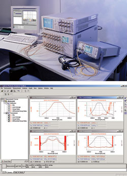
Agilent’s Photonic Foundation Library synchronizes test and
measurement components to optimize performance and reduce sampling times.
Agilent’s Photonic Foundation
Library is one attempt to distill the expert knowledge behind such feats into a
package suitable for all.
“With the analysis tool kit,
the user interface, we provide usability, especially to novice users who don’t
want to program, who cannot program and who don’t even have a compiler. They
just want to use the equipment,” Löffler said.
He added that engineers who have no
time for programming are another target group for the product.
Below the line
Software, of course, continues to extend the capabilities
of the hardware behind the semiconductor industry. Moore’s law states that
the transistor count of an integrated circuit doubles every 18 months, driven partially
by increasing chip size and partially by the technological ability to cram more
transistors into every chip. The combined effect is increasingly powerful and inexpensive
electronics.
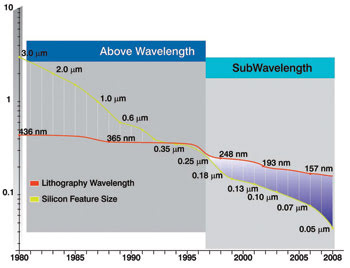
To keep up with Moore’s law, semiconductor manufacturers must photolithographically define features that are smaller than the wavelength of the exposing radiation. Courtesy of Numerical Technologies Inc.
Putting more transistors on a chip
has required smaller transistors, and the industry talks in terms of nodes or generations,
referring to the size of the electronic gates necessary to enable such chips. Until
a few years ago, the gates were larger than the wavelength of the radiation used
to image them photolithographically on a semiconductor wafer. That is no longer
the case.
Today’s state-of-the-art manufacturing
is pushing 110-nm features that are imaged with 193-nm radiation. This gap is not
going away, and it presents a host of problems. Through the use of proprietary software
and other techniques, however, Numerical Technologies is providing industry leaders
such as chip maker Intel, stepper maker Nikon and mask maker Dai Nippon Printing
with the tools to overcome these difficulties.
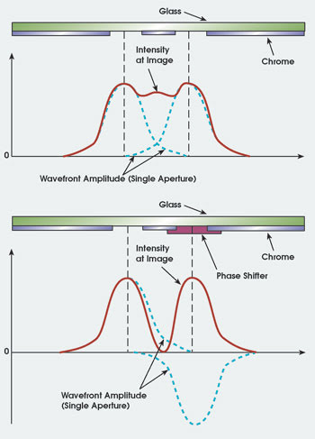
Phase-shifting masks alter the exposure wavefront on target, enablingsemiconductor manufacturers to achieve subwavelength feature sizes. Courtesy of Numerical Technologies.
The relationship between Numerical
Technologies and its clients ranges from supplying products and services to engaging
in joint developments and alliances. The company’s tactics include an automated
method for producing and exploiting a phase-shifted mask, taking advantage of destructive
interference by putting two adjacent regions 180° out of phase with each other.
This can, for example, create a dark space between what would otherwise be two overlapping
light regions.
The intelligent employment of phase
shifting enables the effective resolution to be half the exposing wavelength. Through
the use of optical proximity correction, the company’s approach anticipates
printed distortion in such locations as corners or at the ends of bars. The software
then alters the design in such a manner as to remove part of the distortion on target
and to allow the pattern to print as desired.
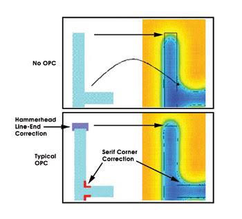
Optical proximity correction for
semiconductor manufacturing anticipates the distortion that occurs in corners or
at the ends of bars. Software alters the circuit design, introducing other, deliberate
distortion so the pattern will print as desired. Courtesy of Numerical Technologies.
“Basically, in order to achieve
the features that the designers have placed in their design, you need to correct
for light that is either not there or that is too much,” Weed said. “It’s
wavelength engineering.”
Weed explained that the corrections
are based on the measurements of a processed test pattern. The corrections then
bubble up through the fabrication process, the photomask making and layout. Only
the basic electrical design remains unaffected. What finally is etched on the photomask
and printed on a wafer may be very different from what the designer specified electrically,
but the chip will perform closer to the original intent than it would have done
otherwise.
Software plays a role in other aspects
of front-end semiconductor manufacturing. “You have to do things to the lens
that are really more than perfect imaging,” said John Wiesner, senior vice
president for engineering at Nikon Precision Inc. in Belmont, Calif. The company
is the North American sales and service arm for its Japanese parent, one of the
leading makers of semiconductor photolithographic tools.
Calibrated imperfections
To produce the calibrated imperfections necessary
to achieve the desired results on-chip, companies like Nikon start with sophisticated
software in the lens design. According to Wiesner, this involves much more than
ray tracing. The software employs physical optics wavefront-propagation algorithms
in painstaking computations that calculate and model an image as it propagates through
the lithography system.
To do so, a phase-measuring interferometer
first monitors the characteristics of radiation passing through a stepper and related
components. The software then extracts the first 37 Zernike coefficients. This information
enables the manufacturer to adjust the illumination, numerical aperture and other
parameters to improve the system’s optical performance for a given type of
image without running a series of experiments.
Nikon also has introduced a software
technique that allows the adjustment of lens imaging and illumination properties
beyond the tuning of focus, numerical aperture and sigma so that its products can
be optimized for particular imaging requirements. Wiesner noted that, although intelligence
and finagling can overcome some of the constraints of physics and engineering, a
perfect design for the lenses in a stepper, for example, is insufficient to realize
the demands of today and tomorrow.
“They have to be essentially
better than perfect, because they have to do things that the lens wasn’t necessarily
designed to do.