Hamamatsu Corporation Wins Circle of Excellence Award
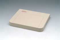
C7930DP Flat Panel Sensor
 Manufactured from a single 12-in. silicon wafer using conventional CMOS processes, the C7930DP flat panel sensor was developed by Hamamatsu Corp. of Bridgewater, N.J., for low-energy mammography, biopsy and traditional nondestructive test applications. The sensor is designed with the scintillator deposited directly on its surface, making it suitable for digital radiography.
The compact sensor has 4416 X 3520 50-µm pixels, measures 220.8 X 176 mm and has a 282.4-mm diagonal. The amplifiers and shift registers are integrated on the same chip, with the amplifiers at the bottom of each vertical column, requiring 4416 charge-sensitive preamplifiers. The sensor converts the optical signal produced by the x-ray scintillator into an electrical signal at the photodiode, where it is stored as charge.
The digital shift register turns on a switch that connects each diode in the row to its corresponding video line. The charge travels down the video line to the amplifier at the bottom of the column, and each row is read individually, with the process repeated 3520 times.
The system comprises signal-processing electronics, analog-to-digital converters and timing generators. An RS-422 digital video output facilitates connection to signal-processing systems.
/Buyers_Guide/Hamamatsu_Corporation/c5841