Graphene on Chip Closing the Gap with Germanium
VIENNA, CAMBRIDGE, Mass., & HONG KONG, Sept. 17, 2013 — Graphene-based photodetectors can efficiently convert infrared light into electrical signals, three independent studies report this week. The work "makes it very likely that graphene will soon replace germanium and compound semiconductors in high-performance light detectors," said editors at Nature Photonics, which published all three papers.

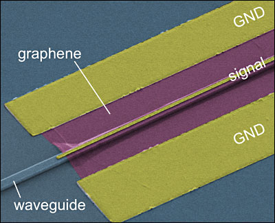
The light signal arrives through a waveguide (left), in the 2-µm-wide graphene sheet, electrical current is generated. Courtesy of TU Vienna.
Graphene — a single layer of carbon atoms arranged in a honeycomb lattice — with its exceptional electrical and optical properties, is being pursued as a more attractive alternative to germanium or compound semiconductors for silicon-based photonics. Attempts to integrate photodetectors made of materials such as germanium onto a chip have resulted in bandgap-limited detectors that can process light of only a specific wavelength range. But graphene — a zero-bandgap material — has been shown to convert all wavelengths used in telecommunications equally well, and recent graphene integration work has yielded high-performance optoelectronic devices such as modulators, polarizers and photodetectors.
All three of the new papers appear this week. Dirk Englund and colleagues from Columbia University, MIT and the IBM T.J. Watson Research Center report an ultrafast graphene light detector with a responsivity about 16 times greater than that of previous graphene-based detectors over a broad bandwidth of 1.45 to 1.59 µm. Although that amount of current still lags behind germanium photodetectors, “The gap is closing very, very quickly,” Englund told Nature.

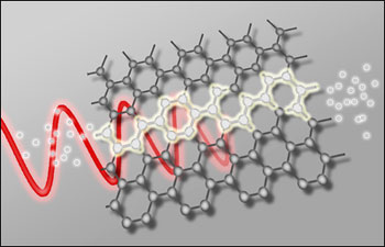
Graphene — a two-dimensional sheet made of carbon atoms — can convert light into electrical current. Courtesy of TU Vienna.
Thomas Müller and co-workers at Vienna University of Technology, working with teammates from the Johannes Kepler University in Linz, describe a graphene light detector with multigigahertz operation for a wide range (1.31 to 1.65 µm) that includes all the bands used by optical fiber communication systems. Its responsivity is about eight times higher than that of earlier graphene light detectors.
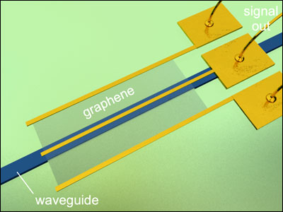
"A narrow waveguide with a diameter of about 200 by 500 nanometers carries the optical signal to the graphene layer. There the light is converted into an electrical signal, which can then be processed in the chip," Müller said.
Two years ago, Müller's team at the university's Institute of Photonics demonstrated that graphene is ideally suited to turn light into electrical current.
"There are many materials that can transform light into electrical signals, but graphene allows for a particularly fast conversion," Müller said.

Visualization of a waveguide-integrated graphene photodetector. Light propagates along the waveguide and is converted in a sheet of graphene into an electrical signal. Courtesy of Thomas Müller.
Not only is his photodetector extremely fast, but it can also be built extremely compact, with 20,000 detectors fitting onto a single chip with a surface area of 1 sq cm. In theory, such a chip could receive data separately through each of those 20,000 channels.
Xiaomu Wang and colleagues at The Chinese University of Hong Kong report on fabricating a high-responsivity graphene photodiode that operates at mid-infrared frequencies, with potential applications in environmental monitoring and on-chip infrared spectroscopy for medical testing.

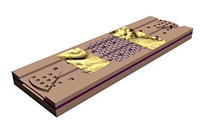
Graphene/silicon hererostructure photodetector embedded in a silicon mid-infrared (2.75 µm) waveguide. Courtesy of Jian-Bin Xu and Xiaomu Wang.
"In addition to having a very wide wavelength detection range, high-speed operation, a low dark current, a good internal quantum efficiency and a small device footprint, this emerging technology also benefits from the mass production of graphene film and its compatibility with CMOS and other aspects of the mature silicon industry," wrote Ming Liu and Xiang Zhang of the University of California, Berkeley, in a News & Views article in Nature Photonics accompanying the research.
For more information, visit: Columbia/MIT/IBM paper or Vienna/Johannes Kepler paper or The Chinese University of Hong Kong paper.
Published: September 2013