Thin germanium layers on silicon may finally give Group IV optoelectronics the performance of the best III-V devices.
David A.B. Miller, Stanford University
Silicon electronics technology dominates information processing and offers a remarkable way to make very complex systems for very little cost. Many of the waveguide passive optical components used today in telecommunications such as wavelength splitters use the same technology base as silicon electronics — the silicon, silicon dioxide and silicon nitride that are the semiconductors and insulators of electronics become the waveguides of optics. Having one platform that could integrate electronics, optics and optoelectronics is an attractive idea, and if possible, the platform could transform the way that photonics technology is applied. However, silicon technology has a major weakness: It does not have strong optoelectronic effects that can be used to emit or modulate light. The mechanisms in silicon are very weak compared with those routinely used in optoelectronic devices made from the III-V semiconductors such as GaAs, InP and InGaAs. This weakness makes it difficult to put information onto light beams using silicon structures, whether for telecommunications applications or for emerging applications such as dense optical interconnects.
The III-V materials are difficult to integrate with silicon for a number of reasons, not the least of which is that they are the dopants that make silicon conducting. Other Group IV materials such as germanium, which is routinely integrated with silicon in modern electronics, might be tried, but none of those Group IV materials shares the same “direct gap” physics exploited routinely in III-V optoelectronics.
Despite the absence of any strong microscopic mechanism in silicon, the other attractions of silicon as a platform are compelling; as a result, there has been impressive work using high-Q resonators or long structures to make optical modulators that can exploit the weak effects in silicon (in particular, the carrier density dependence of refractive index). Silicon photonics as a research field has shown strong progress.1 This technology is being commercialized by a number of companies, including Luxtera Inc. of Carlsbad, Calif., which has succeeded in integrating the silicon photonics technology with silicon electronic integrated circuits. However, there is no doubt that it would be preferable to have the much stronger mechanisms of III-V materials to make compact, high-speed, low-power devices. The engineering freedom that strong effects provide would allow the design of devices without high-Q resonators, thus avoiding their associated fabrication challenges, and precise temperature and tuning requirements.
There are two fundamental approaches to imposing information onto light beams: modulating the laser itself (by modulating its output power) or externally modulating the steady power emitted by the laser. The use of modulators rather than direct modulation of lasers has several advantages, including reducing “chirp” (undesired sweeping of the wavelength under modulation) and avoiding limits on the modulation speed of lasers.
Integrating modulators
When considering integration with electronics and/or dense arrays of optoelectronic devices, modulators have several further advantages. In particular, the additional power required to run the laser is not consumed on the chip, which reduces on-chip power dissipation, and the laser wavelength, power and mode structure can be set and controlled away from the hostile environment of the chip with its high and widely varying temperatures. Especially if the modulator is not a finely tuned resonant structure, precise temperature control is not required on the chip. Although it is sometimes presumed that a silicon laser is a necessary breakthrough for usable silicon photonics, a good modulator may be more important because there is no need to generate the optical power on the chip. After all, electronic transistors do not generate electrical power; they merely modulate electrical power from elsewhere.
One major approach used in telecommunications to impose information onto light beams in III-V structures is the quantum-confined Stark effect.2 As any physics undergraduate knows, the (ordinary) Stark effect is a shift in an atom or molecule’s energy levels as a result of an applied electric field. The quantum-confined Stark effect is an advanced version of this shift that can be seen in the energy levels of a quantum well resulting from an applied electric field. The fundamental concept behind using the quantum-confined Stark effect as the basis for a modulator is that the absorption in a quantum well at a given wavelength can be charged by applying an external electric field.
Because Group IV materials such as silicon and germanium have indirect bandgaps and because the quantum-confined Stark effect had until recently been seen only in direct-gap semiconductors, there still would not be a strong modulation mechanism for Group IV materials. Recently, however, we observed the quantum-confined Stark effect in germanium quantum wells grown on silicon substrates.3-5 The key point is that this effect can be seen at the direct gap of germanium, though there is a lower indirect gap with additional weak optical absorption.

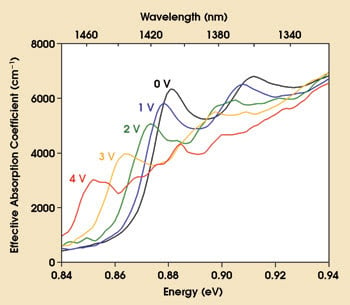
Figure 1. The absorption spectra of Ge quantum wells on silicon substrates are a function of reverse bias on the diode structure containing the quantum well layers.
The typical spectra in Figure 1 show the clear shift of a strong optical absorption edge to lower photon energies (longer wavelengths), typical of the quantum-confined Stark effect. In a further surprise, these spectra are at least as clear and strong as good quantum-confined Stark effect in III-V materials at similar wavelengths. Finally, in a Group IV structure, we observed optoelectronic modulation physics that is as good as — or possibly even better than — that in III-V materials. These structures also have been demonstrated to work in the C-band telecommunications wavelengths near 1.55 μm and at the temperatures of operation of high-performance silicon electronic chips; e.g., 90° C.4
Very recently, we demonstrated the first optical modulators using this approach.5 As is typical with quantum-confined Stark effect modulators, these are reverse-biased diodes. The reverse biasing allows the necessary electric field to be applied without the large currents that otherwise would flow in a semiconductor. Various forms are possible for quantum-confined Stark effect modulators, including waveguides and “surface normal” devices; i.e., with the light propagating perpendicular to the surface, rather than parallel to it as in a waveguide. Moreover, quantum-confined Stark effect modulators can be configured as resonators, or not. Because the quantum-confined Stark effect in the germanium quantum wells is at least as strong as that in the III-V materials, we expect all of these structures to be possible.

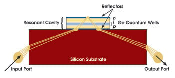
Figure 2. The quantum wells of this side-entry quantum-confined Stark effect modulator are contained within an intrinsic (i) region of a p-i-n diode that also forms a low-Q resonator structure. The diode is reverse-biased to operate the device. (This schematic diagram is not to scale.)
The first working devices used a novel side-entry configuration (Figure 2). In this particular device, light enters and exits through the sides of the silicon substrate wafer, leaving the top surface of the wafer free for electrical connections and the bottom free for heat removal, as is common on silicon integrated circuits. The top surface is a metal mirror, and a second mirror is formed by the interface between the silicon substrate and the SiGe n-i-p diode region as a result of the refractive index difference between the substrate and the diode region. The light bounces up and down within this low-Q resonator, effectively giving it a long enough path through the quantum well region in the middle of the diode for substantial absorption. This particular approach, in contrast to waveguide structures, gives a modulator with a very large misalignment tolerance. To run the modulator, a voltage is applied between the top n layer and the substrate. This first device showed a contrast ratio of 7.3 dB at a 1457-nm wavelength, and the incident beam could be moved laterally over 80 μm while still showing usable modulation.5
With this discovery of quantum-confined Stark effect electroabsorption in germanium quantum wells grown on silicon, the prospects for a fully functional, high-performance platform for electronics, optics and optoelectronics, all potentially integrated on one chip, appear to have taken a major step forward. The result may be lower cost as well as smarter and higher-performance optoelectronics for telecommunications and networks, along with new generations of dense low-power optoelectronics for computer interconnects.
Meet the author
David A.B. Miller is the W.M. Keck Foundation Professor of Electrical Engineering at Stanford University in California. He is director of the solid-state and photonics laboratory and co-director of the photonics research center, both at Stanford, e-mail: [email protected].
References
1. See, e.g., issue on silicon photonics (November/December 2006). IEEE J SEL TOP QUANTUM ELECTRON, Volume 12, Issue 6, Part 2.
2. D.A.B. Miller et al (July 1985). Electric field dependence of optical absorption near the band gap of quantum-well structures. PHYS REV B, 32, pp. 1043-1060.
3. Y.-H. Kuo et al (Oct. 27, 2005). Strong quantum-confined Stark effect in germanium quantum-well structures on silicon. NATURE, pp. 1334-1336.
4. Y.-H. Kuo et al (November/December 2006). Quantum-confined Stark effect in Ge/SiGe quantum wells on Si for optical modulators, IEEE J SEL TOP QUANTUM ELECTRON, pp. 1503-1513.
5. J.E. Roth et al (April 27, 2007). Optical modulator on silicon employing germanium quantum wells. OPT EXPRESS, pp. 5851-5859.
6. D.A.B. Miller (June 2000). Rationale and challenges for optical interconnects to electronic chips, PROC IEEE, pp. 728-749.
Direct and Indirect Gaps
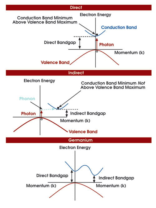
The “direct gap” physics of semiconductor materials is often described in a so-called “band structure,” in which the energies of the various possible electron states in the material are plotted as a function of their (effective) momentum hk, where h is Planck’s constant divided by 2π (~1.054 × 10⁻³⁴ Js) or, more commonly, just as a function of the “wave vector” k. On such a diagram, the states group into “bands” that appear as lines (or surfaces). Although the states appear as continuous lines, they actually are composed of very closely and equally spaced points or states. The most important sets of states for describing semiconductors are the highest “valence” band, in which every state is occupied by an electron in the pure semiconductor, and the lowest “conduction” band, in which every state is correspondingly empty.
In a “direct gap” semiconductor, the lowest point in the conduction band lies directly above the highest point in the valence band. Most of the III-V materials in use for optoelectronics are direct-gap semiconductors. The Group IV materials silicon and germanium, which are from Group IV of the periodic table, both are “indirect gap” semiconductors. In an indirect gap semiconductor, the lowest point in the conduction band is not directly above the highest point in the valence band (Figure 3).

Figure 3. This illustration shows the band structure of direct and indirect gap semiconductors and of germanium.
For making electronic devices such as transistors, it is relatively unimportant whether a semiconductor is indirect or direct. However, for optoelectronic devices, the difference is crucial because a photon has negligible momentum when viewed on the scale of a semiconductor band diagram.
A simple “direct” optical absorption transition in which a photon is absorbed can be viewed as taking an electron from the valence band and placing it in the corresponding state directly (or “vertically”) above in the conduction band, with the energy separation of the states corresponding to the photon energy hv, where h is Planck’s constant, and v is the frequency of the light. The opposite process — in which an electron falls from the conduction band to an empty state in the valence band essentially directly beneath it — generates a photon and is the principal light-generating mechanism in all semiconductor lasers and in most light-emitting diodes. Such direct processes are strong, both in absorption and emission.
But the corresponding processes for absorption and emission across the indirect gap are much weaker. Such indirect transitions cannot take place with only a photon because momentum must be conserved, and a photon cannot provide — or absorb — the momentum difference across an indirect bandgap. A “phonon” — the quantum mechanical particle associated with the vibrations of the crystal lattice — is required to conserve momentum. Such indirect processes are much weaker, and this weakness is the main reason why indirect semiconductors do not make good light emitters. If we place electrons in the conduction band, they will fall to the lowest energy point in the conduction band; the corresponding “holes” — absences of electrons — in the valence band will rise to the highest point, just like bubbles rising towards the surface of water. In a direct gap semiconductor, these “pools” of carriers — electrons and holes — will be directly above one another, and strong direct optical emission can occur. In an indirect semiconductor, however, only the weaker indirect emission is possible, resulting generally in poor light emitters and in weak absorbers near the indirect gap.
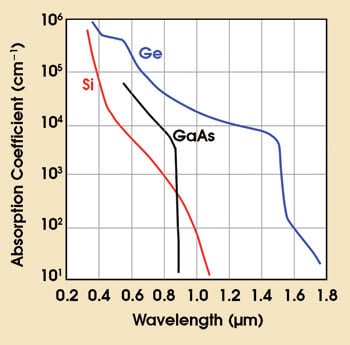
Germanium is an indirect gap semiconductor, but it also has a direct gap at slightly higher photon energy. Though it still does not solve the problem of efficient optical emission, it does show strong, direct optical absorption that rises strongly near the 1.5-μm wavelength, and with a weaker indirect optical absorption tail at longer wavelengths (lower photon energies).

Figure 4. Optical absorption spectra for silicon, gallium arsenide and germanium are shown. Gallium arsenide shows a strong direct absorption edge at about 0.87 μm. Germanium shows a strong direct absorption edge near 1.55 μm and a weaker indirect absorption tail extending to longer wavelengths. Silicon shows a weak indirect absorption tail into the infrared wavelengths and does not show comparably strong absorption until well into the visible spectrum.
The direct absorption can be used for photodetectors and is used here also for modulators in quantum well structures. The physics of the direct absorption in germanium is identical to that in the III-V semiconductors. Figure 4 shows the resulting optical absorption spectra.