Data centers and high-performance computing need faster, less costly and more energy-efficient communication, attributes increasingly difficult to achieve with copper connections. Where distances hover around a kilometer or so, and cost must remain low, silicon photonics could be the answer for today’s data center bottlenecks.
The opportunity for and challenge of silicon photonics lies in data centers and high-performance computing.
An example was on display at an Optical Fiber Conference panel session held in Los Angeles last year. According to Yuval Bachar, at the time a hardware networking engineer at Facebook, the company’s data centers grow two- or threefold every eight to 10 months. As a result, Bachar was looking to silicon photonics as a way to move from 100 to 400 to 1000+ gigabits per second (Gbps) networking, stepping up every 12 to 18 months.
As this discussion revealed, increasing use of optical links in data centers and high-performance computing looms, providing performance and production increases while costs decline. Given that, device sales will move from less than $25 million in 2013 to more than $700 million by 2024, said Eric Mounier, who heads silicon photonics market analysis for Yole Développement.
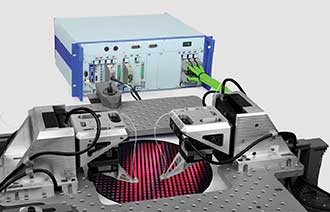
Economical silicon photonics manufacturing demands fast and automated alignment during assembly and testing. Here 3-axis alignment is used for planar wafer test. Courtesy of Physik Instrumente.
The reasons for this opportunity arise from the explosive growth in electricity usage by data centers. In America alone, they consumed an estimated 91 billion kilowatt hours in 2013, a figure that is expected to grow to 140 billion — a more than 50 percent increase — by 2020, according to the National Resources Defense Council. The need to reduce power consumption is so great that large data center operators are turning to novel solutions. Microsoft Corp., for instance, is testing putting data centers under water to save power by cutting air-conditioned cooling.
Part of the problem is that pushing electrons rapidly down copper wires takes energy, a factor that can be eliminated by using light to carry information instead. But, existing optical solutions are limited in distance and bandwidth, leaving an opening for a new approach. “Silicon photonics seems to be the short-term solution to face the future interconnect bottlenecks for data centers,” Mounier said.
Facebook’s target is a dollar per gigabit for 100 Gbps speeds over a single mode fiber for distances of 500 meters. Achieving that requires a more than doubling in multiple performance measures while cutting costs significantly, which demands advances in photonics chips and packaging. Improvements in the latter are particularly important because packaging contributes up to 80 percent of the cost of a component, according to Yole analyst Claire Troadec.
Searching for alignment
Additional challenges are presented by planned innovations, such as putting sources and optics closer to or even on electronic chips. “Because integration also includes a laser source and the optics is getting closer to the electronics, heat dissipation will also become an issue,” Troadec said.
Recent developments promise solutions. On the testing and packaging fronts, Physik Instrumente GmbH & Co. KG, based in Karlsruhe, Germany, has developed an alignment engine that enables nanoscale accurate, multi-degree-of-freedom global optimization of the placement of fibers and other photonic components, said Scott Jordan, senior director of nanoautomation technologies.
Thanks to a new digital gradient search technique that rapidly finds the best possible consensus alignment across multiple couplings in one step, tasks can now be completed in a fraction of the time it used to take, which boosts throughput and cuts costs, according to Jordan. He added that more importantly the increase in capabilities enables cost-effective testing and binning into good/bad, high/low or other device capability categories.
“You have to test them. You have to qualify them. You can’t just bring electric probes in contact with the wafer anymore,” Jordan said.

A 200-mm wafer with dies bonded on it, prior to the lasers being transferred to and bonded to a wafer with silicon photonics chips. Courtesy of CEA-Leti.
The desire to make alignment and packaging easy and inexpensive also explains some of the silicon photonics design decisions and associated innovations made by optical and electrical interconnect maker Mellanox Technologies Inc., according to Arlon Martin, senior director of interconnect marketing. For example, the Sunnyvale, Calif.-based company’s products have three micron-wide waveguides, several times larger than those used by competitors. The bigger size was chosen because it allows low loss transmission of a broad range of wavelengths and the beam profile of most lasers is the same width, enabling direct coupling, Martin said. He added that the wider waveguides also more easily connect to standard single mode fiber.
But, a bigger waveguide limits the speed of germanium-based detectors and modulators. That’s why Mellanox narrows the critical dimension of such structures to less than a micron, opting to do so in a cost-effective manner.
“We set the width with a mask set. So we’re leveraging what the semiconductor industry is extremely good at,” Martin said. “It allows us easily to scale to the next generation, which will be 50-Gbps devices.”
Optical interconnects have to mesh with their electrical counterparts, which dominate the short runs found inside computer racks. For that reason, the least expensive overall solution is when the speed of the two technologies match, and that will continue to be true for the foreseeable future, Martin said.
Another reality impacting the future arises from the nature of silicon and germanium, the two semiconductors used in silicon photonics. They are indirect bandgap materials and so cannot lase as well as can be done by a III-V combination semiconductor, such as indium phosphide (InP) or gallium arsenide (GaAs), said Sylvie Menezo, director of the nanoelectronic silicon photonics program at France’s technological research institute CEA-Leti.
But in all other components — waveguides, modulators, photodetectors and more — silicon photonics today is up to the task, according to Menezo. IRT Nanoelec is a research program headed by CEA-Leti, working with industrial partners Mentor Graphics Corp. of Wilsonville, Ore., STMicroelectronics of Geneva and SAMTEC Inc. of New Albany, Ind. In particular, the project addresses packaging-related problems of aligning single mode fibers and coupling lasers with silicon photonics chips.
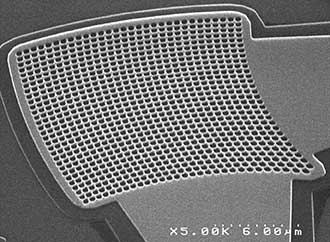
A surface grating coupler that couples light from a fiber sits atop a silicon photonics chip. Courtesy of CEA-Leti.
For the laser issue, Menezo said one solution is to use InP or other III-V chips, place them atop an intermediate wafer, and then bond them onto a similarly sized silicon wafer. This is economical, in part, because at roughly 100 microns the alignment requirements are very loose, at least in terms of nanoelectronics. In that realm, a human hair, which is about the same size as the alignment tolerance, is huge.
Another cost savings comes from reducing waste. “Putting the expensive III-V compound semiconductor material only where needed — at the location of lasers — saves on cost, as does doing the laser processing at the wafer level. In addition, we think that our laser is likely not to require any hermetic package,” Menezo said in listing cost-saving attributes.
As for alignment of fibers, Menezo said it’s critical that it be done at the photonic chip surface because that enables testing at the wafer level. This is early in the manufacturing process and key to reducing overall costs. To support this and a reduction in alignment expenses, IRT Nanoelec has developed a 3D toolbox to help speed passive, and therefore inexpensive, alignment.
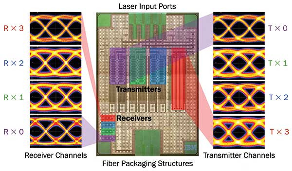
A silicon photonics chip that contains all electronics and photonics, except for the laser source, could someday form the basis for 25-gigabits-per-second-per-wavelength data communication. Courtesy of IBM.
Electronic and photonics on a single chip
Another performance-enhancing yet cost-reducing innovation comes courtesy of IBM Corp. In March 2015, the Armonk, N.Y.-based technology company announced an integrated silicon photonics technology for wavelength division multiplexed data communications. This contained all the electronics and photonics, aside from the laser source, on a single chip, a possible basis for optical interconnects that run at 25 Gbps per wavelength. It also puts the conversion from electrical to optical closer than ever to the chip itself.
That advance is only part of the company’s silicon photonics efforts, according to Will Green, manager of the silicon integrated nanophotonics group at IBM Research. “We have developed wafer-level optical and mechanical structures that permit optical fiber or III-V lasers to be directly attached to the chip,” he said.
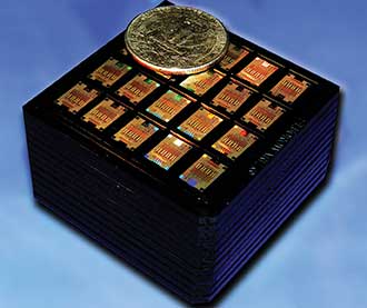
Integrated silicon photonics demonstration chips. Courtesy of IBM.
Green added, “These optical and mechanical features facilitate photonic assembly techniques using passive self-alignment of the packaged component to the silicon photonics chip.”
A plus is that the structures and the packaging they enable are compatible with conventional microelectronics assembly tooling. Thus, it might be possible to eliminate most — if not all — manual assembly, a further cost savings.
In another advance, Wei Shi, an assistant electrical and computer engineering professor at Université Laval in Quebec City, recently demonstrated a tunable optical filter manufactured with CMOS-compatible nanostructures. The research appeared in an Optics Letters paper.
Tunable filters are essential to flexible optical networks that allocate spectrum as needed, Shi said. “They give a network controller the freedom to select the frequency and bandwidth for each channel and change them on the fly.”
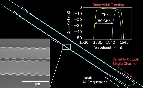
A tunable filter, potentially useful in next-generation optical communication networks based on advanced silicon photonics chips. Courtesy of Wei Shi, Université Laval.
The researchers fabricated 10-nanometer structures into gratings with a pitch about half a wavelength of the light being used, or 300 nanometers. They then selectively heated the structures, altering their optical characteristics. The result was a rapid and significant shift in filter performance.
The goal of the research is to eventually develop an integrated silicon photonics chip with this technology. This could then be important for next generation coherent optical transmission systems, Shi said. He added it may take up to five years to actually deliver mass production products based on this technique.
These and other developments indicate the potential of silicon photonics to hit cost and performance goals. Today low-cost but low-performing optical devices rule when runs are less than 300 meters; more expensive but higher-performing ones dominate when spans are more than 10 kilometers, said Jean-Marc Verdiell, CTO of the optical group at SAMTEC. That leaves silicon photonics in the middle: data centers and high-performance computing where distances are a kilometer or so but cost has to remain low.
One of the IRT Nanoelecs industrial partners, SAMTEC, is a transceiver maker. The company integrates silicon photonics, electronic chips and fiber into a single packaged component that can transmit and receive optical signals.
In electronics, an integrated part almost always outperforms a solution-based on discrete components in performance, price and power consumption, according to Verdiell. In contrast, he added, silicon photonics integration leads to performance trade-offs. The hope is that efforts underway will change this integration dynamic and make silicon photonics more like electronics in that regard.
For now, Facebook and others confronting high demands are turning to the new technology for its long-term appeal. As Verdiell said, “In the beginning, silicon photonics cannot compete on cost alone. There has to be a performance or functionality element to justify it.”