Silicon photonic wire waveguide sensors detect the presence of pathogens and chemicals.
Siegfried Janz, National Research Council of Canada
Molecular sensors can detect trace amounts of molecules present in food and water that signal the presence of danger to humans. The target may be the toxic molecule itself, as in the case of pesticide residues and pollutants, or it may be a biomarker molecule — such as DNA or an antigen — that is associated with pathogenic organisms.
The ideal sensor should detect the lowest possible level of toxin and should register a highly specific response to minimize the possibility of false negative readings, which can be disastrous. The device also should minimize false positives that might trigger needless and expensive countermeasures. To reduce test time and cost, transduction methods requiring a minimum of sample processing should be used — hence the strong interest in direct label-free detection, which requires no prior attachment of fluorescent or other tags to the sample molecules.
With that in mind, scientists at the National Research Council of Canada recently demonstrated that silicon photonic wire evanescent field waveguide sensors can overcome the limitations of other evanescent field waveguide sensors.
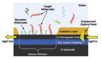
In a traditional evanescent field waveguide sensor designed for label-free molecular sensing, the evanescent light extends a short distance outside the waveguide core and interacts with the material above the waveguide’s surface (Figure 1). As a result, the sensor waveguide’s effective index and, therefore, the phase velocity of light propagating in the sensor waveguide depend on the refractive index just above the surface. They will shift with changes in local analyte liquid chemical composition or whenever molecules bind directly onto the waveguide surface. The resulting propagation delay is measurable with very high accuracy using any one of several interferometric methods.

Figure 1. An evanescent field waveguide sensor is shown on a silicon-on-insulator wafer. When target molecules bind to the receptor molecules in the sensor window, the change in local refractive index is felt by the evanescent tail of the optical waveguide mode and shifts the phase velocity of the guided light.
For all refractive index sensors, the minimum measurable index change scales with the ratio between the sensor interaction length and the wavelength.1 This is the optical analog of the Heisenberg uncertainty principle encountered in quantum measurement of momentum and position. The index is, in effect, obtained by measuring the wave vector or momentum of a photon.
This optical uncertainty principle forces a compromise between the minimum level of detection and the sensor size. Moreover, the interaction length may be limited by attenuation of the optical excitation itself, as in the case for surface plasmon resonance sensors, the most widely used label-free molecular sensor. In surface plasmon resonance, the sensitivity is fundamentally limited by the effective interaction length of only a few tens of microns, the distance over which plasmons propagate before being absorbed by the metal.
The transduction signal in evanescent field waveguide sensors is a cumulative optical phase delay. Unlike with surface plasmon resonance sensors, the response may be increased nearly indefinitely simply by extending the sensor waveguide length because the propagation distance of light in a waveguide is unlimited.
However, using very long waveguide paths to achieve high sensitivity can be incompatible with the small sensor size and spotting technologies needed for practical multiple sensor biochip arrays. In most applications, the ability to array multiple sensors to test for nonspecific binding and to provide redundancy checks is essential to achieve acceptable reliability.
In addition, sensors with high response to molecular adsorption often are extremely sensitive to fluctuations of environmental variables such as temperature, which limits their usefulness outside a carefully controlled environment.
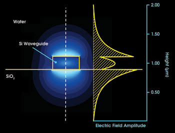
The silicon photonic wire evanescent field waveguide sensors that the National Research Council scientists developed use a waveguide formed in a 220-nm-thick silicon layer on a silicon-on-insulator wafer (Figure 2).2,3 Apart from their extremely small size, silicon photonic wire evanescent field sensors have advantages that arise from the large difference between the refractive index of the silicon waveguide core (n = 3.47 at λ = 1550 nm) and that of the surrounding medium (n = 1.32 for water).

Figure 2. A cross section of a 220 × 450-nm silicon photonic wire waveguide and the optical electric field distribution of the vertically polarized mode is shown on the left. A line scan across the center of the waveguide is shown on the right. Most of the optical power propagates in the evanescent tail region adjacent to the waveguide surface.
As a result, for the vertically polarized or transverse magnetic optical mode, most of the light propagates in the evanescent tails that are just outside the surface of the waveguides, rather than in the waveguide core. The evanescent light nevertheless remains confined to a layer extending only about 100 nm into the liquid above the surface, with the result that light propagating in these silicon waveguides has an extremely high optical coupling with molecules at the surface.
At the same time, photonic wire sensor designs can use curved waveguides with bend radii as small as 5 μm, with no loss. The waveguide bend radius in conventional glass waveguide devices must be about 1000 times larger.
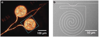
This property allowed scientists to fold photonic wire evanescent field sensors into serpentine paths that occupy a silicon chip area less than 150 μm across but that can contain sensor waveguides longer than 5 mm. Finally, by balancing the sensor element with an identical reference waveguide in a Mach-Zehnder interferometer (Figure 3a), spurious sensor drift resulting from temperature and wavelength fluctuations can be cancelled while the extremely high sensitivity to molecular adsorption is retained.

Figure 3. Shown is an infrared image of a 2-mm-long folded spiral photonic wire evanescent field waveguide sensor in a balanced Mach-Zehnder interferometer circuit, taken while guiding 1550-nm light (a). The dashed square shows the position of the sensor window. A differential measurement between the reference and sensor spirals can eliminate unwanted responses to environmental variables such as temperature. Also shown is an electron microscope image of a 1.3-mm-long spiral sensor in a ring resonator circuit (b).
Photonic wire evanescent field sensors can be incorporated into ring resonator circuits (Figure 3b). Here, the effective sensor interaction length is set by the number of round-trips the light makes while it is trapped in the ring cavity — a number determined by the quality factor of the ring resonator.
The ring sensor allows light to interact with the same molecules every time it makes a round-trip, so that the cumulative response to a finite number of molecules can be much higher than in a one-pass transmission geometry. Incorporating a folded spiral waveguide into the ring sensor shown in Figure 3b further increases the sensor interaction length and improves the diffusion-limited molecular capture probability of the sensor.
The researchers have demonstrated both Mach-Zehnder interferometer and ring sensor devices using biotin-streptavidin protein binding — a well-known benchmark system for establishing molecular sensor performance.
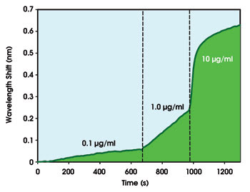
Solutions are delivered to the sensor elements through microfluidic channels in a silicon chip. Biotin molecules attached to the waveguide surface are a very specific receptor for streptavidin, which, if present in solution, binds irreversibly to the biotinylated surface. The resulting perturbation in waveguide phase velocity may be determined from the shifting interference fringes of the Mach-Zehnder output, or from the resonance wavelength shift of the ring resonator (Figure 4).

Figure 4. The molecular binding response from a photonic wire evanescent sensor as a streptavidin protein monolayer forms on the sensor surface, while the streptavidin concentration is increased in one-decade steps. The physical transduction signal is the resonance wavelength shift for the ring resonator sensor in Figure 3b.
At the time of writing, the minimum level of detection for both the rings and the Mach-Zehnder interferometer sensors is less than 0.3 percent of a monolayer of streptavidin protein molecules on the waveguide surface, a value limited by measurement system noise. By balancing the interferometer circuit, as in Figure 3a, the unwanted sensor drift resulting from background temperature fluctuations is reduced to 5 percent of that for a single-sensor element.
The low levels of detection and the reduction in sensor footprint achieved using silicon photonic wire evanescent field sensors are important advances toward optical lab-on-chip molecule-sensing devices based on waveguide evanescent field transduction. Because these sensors can be produced using only a small subset of the CMOS fabrication tool set, sensor chip cost should become negligible, provided there will be a market that warrants wafer-scale production.
One current goal is to develop biochip arrays for label-free real-time monitoring of molecular interactions in genetic, proteomic and drug discovery research. The high sensitivity, small size and overall flexibility of silicon photonic wire evanescent field sensors will permit researchers to access reactions involving smaller molecules, lower binding constants and lower concentrations than are possible with commercial systems such as surface plasmon resonance sensors.
Eventually, application-specific sensor chips will be developed for larger commercial markets for pathogen detection and chemical sensing in the food industry, in environmental monitoring and in diagnostics.
References
1. K. Tiefenthaler and W. Lukosz (February 1989). Sensitivity of grating couplers as integrated-optical chemical sensors. J OPT SOC AM, pp. 209-220.
2. A. Densmore et al (Dec. 1, 2006). A silicon-on-insulator photonic wire based evanescent field sensor. IEEE PHOTON TECHNOL LETT, pp. 2520-2522.
3. A. Densmore et al (2008). Spiral path, high sensitivity silicon photonic wire molecular sensor with temperature independent response, OPT LETT, in press.
Meet the author
Siegfried Janz is group leader of the optoelectronic devices group at the Institute for Microstructural Sciences, a division of the National Research Council of Canada in Montreal; e-mail: [email protected].