
Fluorescence Microscopy: Getting the Picture Right
Camera choice has to strike a balance between certain sensor properties, camera-related topics, and the needs of the intended applications in industry or medicine.
FELIX ASCHE, BASLER AG
Fluorescence microscopy is a very broadly used term covering numerous applications. It ranges from basic life science applications such as time-lapse cell viability assays — in which dead cells are counted as they start to fluoresce by intrusion of a fluorochrome that cannot enter intact living cells — to sophisticated techniques where only very few photons or single molecules are detected and localized by specific high-end hardware and software. It can be quite complex to design an optical imaging system that perfectly fits a specific application. And at the same time, instrument manufacturers are facing pressure to keep the costs down in the medical and life sciences markets.
Optical format and resolution
Looking at the visible wavelength range, the optical setup considerations regarding format, magnification, and resolution do not significantly differ from normal light microscopy applications and are therefore not described here. However, it is important to know that the overall costs increase when larger optical formats such as the F-mount are used. The most common mount is the C-mount, which (with up to 1.1-in. sensors) delivers very good optical performance, as well as most products and solutions at a reasonable price. The smaller S-mount is a good choice when size-restricted and low-cost instruments are developed. Squared sensors are preferred to capture the maximum image content.
Because the sensor takes over a central role in an imaging system, the selection regarding certain performance specifications is of major importance.
CCD, CMOS, sCMOS, and BSI
From its beginning in the late 1970s, CCD (charge-coupled device) technology has been strongly established and is still available in high-end microscopy cameras. Sony, the leading manufacturer of CCDs globally, has discontinued this technology, and instrument manufacturers using CCDs are being forced to find alternative cameras for their systems. The newer CMOS technology has spread through consumer sensor markets for many years and has recently become competitive. Noise levels are now comparable or even better than with the traditional and commonly used CCD sensors, enabling the new technology to deliver higher speed, higher resolution, and less power consumption/heat dissipation at lower prices into medical and life sciences applications.
Scientific CMOS (sCMOS) cameras were introduced in 2010 through the collaboration of three companies working to provide better performance (mainly through faster CMOS-like readout speeds and higher dynamic range) compared to aging CCD technology, which continued to provide a superior noise behavior and brought higher image quality and sensitivity. CMOS sensor development is still rapidly accelerating. Recently, a technology called backside illumination (BSI) found its way into industrial image sensors. BSI significantly improves the pixels’ quantum efficiency. Coming from the smartphone market with its demand for smaller pixels, this technology involved reversing the orientation of the pixel structure to present the light-sensitive photodiode directly below the microlenses. With this design the metal wiring structures no longer inhibit the incident photons, improving the so-called fill factor (the relation of the photoactive and nonphotoactive area) of the pixels (Figure 1).
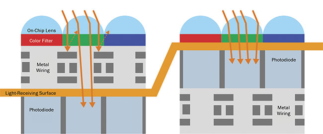
Figure 1. Frontside-illuminated (left) and backside-illuminated pixels (right). Courtesy of Basler AG.
However, BSI sensors can have other additional noise sources contributing to the dark current. Dark current is the leakage of electrons during exposure. This can make these sensors less suitable for longer exposure times. Furthermore, state-of-the-art frontside-illuminated (FSI) sensors can still be a better choice in certain applications, showing excellent performance also in low-light conditions (Figure 2).
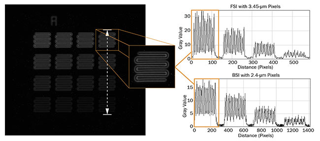
Figure 2. A persistent fluorescence carrier with 8.5-µm small structures of varying intensity was imaged under the same microscopic conditions (same optical path and lighting, and 10-s exposure) with a current BSI (Basler ace acA3088-57um, IMX178) and FSI sensor (Basler MED ace 5.1 MP, IMX250). For the FSI camera, the histogram shows nearly doubled gray values. Courtesy of Basler AG.
Beyond CCD and CMOS, a few additional high-end sensor types are also on the market, such as EMCCD (electron multiplying CCD) and ICCD (intensified CCD). However, these cameras are generally not considered for large products today, as the technology is too expensive and serves mostly niche applications.
CMOS technology will continue to evolve in the years to come; fluorescence microscopy can be expected to be dominated by this state-of-the-art technology in the future, while further developments of traditional CCD technology will tail off. For instrument manufacturers and their current and future products, cameras with CMOS sensors are acknowledged as the better choice.
Monochrome or color
For fluorescence applications, monochrome cameras are usually preferred because of the higher quantum efficiency. The technical factor driving this difference is that in color cameras, Bayer microfilters on each pixel let only certain wavelengths pass through. This filtering is needed to calculate color information of the image using a process called debayering. As the color filters block a certain amount of light, fewer photons reach the photon-reactive area of the pixel. In addition to the Bayer pattern on the sensors, the IR-cut filter in color cameras presents a limiting factor because it blocks light of approximately 650 to 700 nm upward (Figure 3).
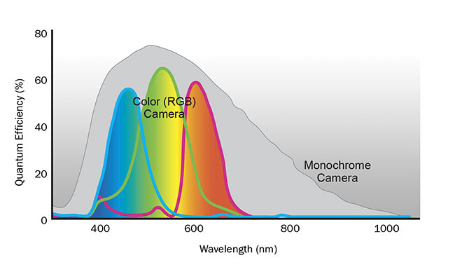
Figure 3. Because of red, green, and blue color filters on the pixels, the quantum efficiency is lower
in a color camera compared to a monochrome camera. In addition, color cameras typically come
with an IR-cut filter blocking light of ~650 to 700 nm upward. Courtesy of Basler AG.
Typically, images with multiple fluorescence markers for specific detection and co-localization of molecules of interest are made from separate images using monochrome cameras. Selectable light sources and filter sets provide the right combination of excitation and emission wavelengths for each fluorophore used (Figure 4).
However, certain applications may create a demand to do color imaging and fluorescence within one instrument using only one camera. This is possible if the sensitivity demands of the fluorescence application are not too high.
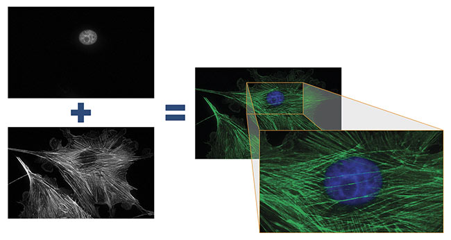
Figure 4. Two fluorescence images of a commercially available BPEA (bovine pulmonary artery
endothelial) cell substrate, taken with a front-illuminated monochrome IMX174 CMOS sensor in a Basler MED ace 2.3 MP mono camera (exposure times: 500 ms DAPI, 5 s Alexa Fluor 488, 63× magnification).
Both single images, showing different cell structures (cell nucleus and filamentous actin), are then
colored by software and merged, showing both structures in one image. Courtesy of Basler AG.
Global and rolling shutters
CCD sensors have only one shutter type (global) while CMOS sensors are available in two types: rolling and global. Choosing the right sensor has a significant impact on image quality, especially when target objects are moving. In rolling shutter sensors, the pixels are exposed line after line. As a result, an object that has changed its position between signal capturing of two lines produces deviating image situations, generating space distortion in the image. A technical advantage of rolling shutter sensors is that they have fewer electronic parts in the pixel, which can result in less noise during readout. Meanwhile, global shutter sensors expose all pixels of the sensor at the same time. In this case, there is no time shift between the exposures of the different pixel lines, thereby generating no space distortions when objects are moving.
Sensitivity and dynamic range
Before taking a closer look at the quality of an image, it is important to ensure that the system is sensitive enough to capture the fluorescence signals, which can be very weak, depending on the individual application. Sensitivity should be understood as the minimum amount of light that is required to generate a signal that can be distinguished from noise. An important value is the quantum efficiency (QE) describing the ratio between the incident photons of the light source and the generated electrons of the pixel. It depends on the wavelength, and to get the best result, the spectrum of a given sensor should fit with the emission spectra of the fluorophores in the application. The higher the QE, the better the yield of photons, enabling shorter exposure times, reducing photo bleaching of fluorophores, and potentially improving overall imaging speed.
Often it is also beneficial to have a wide range of light intensities that can be resolved with one exposure. Here the full well capacity is relevant. It describes the maximum number of electrons that can be generated by one pixel per exposure. The higher the full well capacity, the more light can be captured before a pixel is saturated, reducing the requirement of additional exposures due to saturation.
Combining the maximum number of electrons with the lowest number of electrons required to produce a true signal (see “read noise” in the next section), the dynamic range characterizes a camera’s overall ability to measure and distinguish different levels of light.
Finally, there is the absolute sensitivity threshold, which is the number of photons required by one pixel to generate a signal-to-noise ratio (SNR) of 1 — meaning the signal is equivalent to the noise. The smaller this value, the less light is required to produce a true signal. Because it does not take into account the pixel size, it cannot be directly used to compare two cameras when their pixel sizes are different.
Depending on the quantification requirements of the application and the technical dynamic range of a given camera, the bit depth of the pixel determines the number of gray values that can be differentiated. Typical machine vision cameras have a depth of 8 bit (28 or 256 gray values), which is already sufficient for visual needs, since the human eye can only resolve 6 to 7 bit. Beyond that,
12 bit (212 or 4096 gray values) is common and technically sufficient in the majority of cases. However, certain scientific applications demand 14 or even 16 bit (214/216 or 16,384/65,536 gray values). It is obvious that image file sizes significantly increase with the bit depth, requiring more IT resources for processing and storing; interface bandwidth may also create a bottleneck at even lower frame rates. However, for the majority of cases, the exposure time will probably be the limiting factor that inhibits very fast sensor readouts.
Image quality and noise
Noise is the deviation between the true signal value and the value that is produced by a measuring system. The SNR quantifies the overall noise of an imaging system at a certain light level and is a common parameter used to compare cameras. The higher the SNR, the better the image quality. In the imaging process, there are types of noise that can only rarely — if at all — be reduced by the camera technology (e.g., photon/shot noise, which is caused by the photons’ physical appearance). However, other noise types that influence image quality are significantly affected by the sensor itself and the camera technology. In recent years, the former CCD technology was surpassed in the areas of image quality and performance by modern CMOS sensors. Read noise — or temporal dark noise — is the noise added to a signal per one shutter event and is given in e¯/pixel. Modern CMOS sensors go down to a read noise of only 2 e¯/pixel (Figure 5).
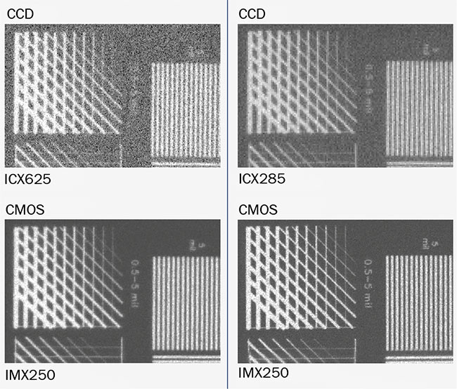
Figure 5. Comparison of the noise behavior (temporal dark noise) of
CCD and CMOS cameras with an exposure time of 10 ms. Courtesy of Basler AG.
Another noise source that is relevant for fluorescence applications becomes important when exposure times increase; it is caused by dark current. Dark current is the leakage of electrons during exposure and is expressed in e¯/pixel/s (Figure 6). As a rule of thumb, the dark current doubles with each temperature increase of 7 °C. Noise types that describe not a temporal- but a space-related behavior are called fixed-pattern noise; this describes deviations that can be seen between different pixels. It can be caused by the pixel electronics or by inconsistent temperatures over the sensor area. Standardized quantification measures of these noise types are the DSNU (dark signal nonuniformity), which describes the deviation of generated electrons without any light signal, and the PRNU (photoresponse nonuniformity), describing the pixel-to-pixel deviation at a certain light level. By setting cutoff values on pixel-to-pixel deviations, one can further differentiate and describe outlying pixels as defect pixels, such as hot pixels, that show high gray values without a corresponding signal. Certain camera manufacturers already correct defect pixels during quality control by interpolation of neighboring pixels so integrators are not impaired by these artifacts.
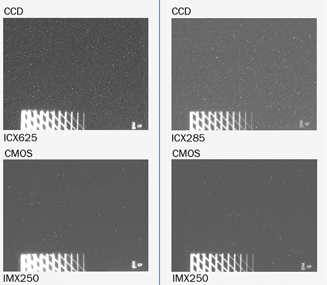
Figure 6. Comparison of the noise behavior (with dark current noise) of CCD and CMOS cameras with an exposure time of 4 s. Courtesy of Basler AG.
There are several different interfaces on the market. To decide which interface is required, one should look at the following points, depending on the individual application: data/image rate, cable length, standardization, integration effort, and costs. The interface technologies USB 3.0 (renamed 3.2 Gen 1) and GigE represent the current state-of-the-art interfaces that are feasible for integration into fluorescence microscopy-based systems. For both interfaces, vision standards are available that provide specifications developed by leading camera manufacturers to improve vision system design, effort, and performance for the camera integrators.
USB 3.2 Gen 1 is the common and
established plug-and-play interface offering the easiest possible integration, enabling data rates of 380 MB/s (e.g.,
75 fps at 5 MP) — sufficient for the majority of applications and with cable lengths of up to a few meters, including power supply, and also supporting multicamera integration. GigE is used when longer cable lengths and a more precise synchronization of multiple cameras is required. The bandwidth of GigE is 3.8× slower (100 MB/s) than that of USB 3.0, but 5 GigE and 10 GigE are becoming available in forms that enable higher data rates of 500 MB/s and 1000 MB/s. For USB 3.0, new versions with up to fourfold higher bandwidth have already been published as well. However, they have not found their way into series vision products as yet.
Integration of new standards typically requires new accessories or peripherals, which adds a delay in availability that can negatively affect time to market because of the limited range of established products.
Cooling
The temperature of the sensor has a central impact on dark current, which decreases the SNR and image quality — especially when light signals are weak and longer exposure times are required. Cooling of cameras is therefore an important topic, but not necessarily mandatory in fluorescence imaging. As cooling measures significantly affect the total cost of ownership, the majority of cameras are only passively cooled, which is already sufficient for applications with strong fluorescence signals. Still, the design of these cameras has an impact on the sensor temperature.
Heat production should be avoided by designing the operation with low power consumption, and heat should be efficiently transported to the outside via the internal hardware design (by the camera manufacturer) and through mounting the camera to a further heat-dissipating carrier (by the camera integrator). For active cooling of the sensor, thermoelectric (Peltier) elements are used, and normally an integrated fan removes the heat that is generated by the Peltier element. The fan also helps to prevent condensation on or freezing of camera parts when their temperatures are below ambient. If vibrations (which can arise from the fan) need to be prevented in the system, some cameras can even be water-cooled. The longer the exposure time, the lower the cooling needs to be. Due to these variabilities, it is not possible to list concisely the conditions of the applications at which cooling measures are actually required. But for many applications it can be assumed that up to levels of several seconds, the noise caused by the dark current of modern high-quality CMOS sensors does not have a significant negative influence.
Beyond the summarized hardware and sensor specifications, cameras can provide firmware features that are designed to improve image quality in low-light conditions.
One example is the defect pixel correction. During the final testing procedures at Basler AG, the camera is tested at different exposure times, and defect pixels are located and saved inside the camera’s cache. In operation mode, the values of defect pixels can be interpolated by the weighted sum of the neighbor pixels. This helps improve image quality and SNR.
Another firmware feature is called “long exposure mode.” In this mode, the camera produces less heat during exposure and thereby runs at a lower internal sensor temperature, enabling a lower noise level. The feature also compensates for sensor glow. In conclusion, checking the availability of firmware features in the manufacturer’s documentation may be helpful for finding the right fluorescence camera.
The current CMOS sensor generations make applications possible that were formerly impossible without the investment of multiple thousands of euros in a CCD camera. These new possibilities become more important as fluorescence becomes an increasingly used tool in the life sciences, making structures and processes visible. And because of the discontinuation of this product group by Sony, the dominant global supplier, manufacturers in the medical and life sciences need to replace the CCD cameras integrated in their instruments. Providing excellent performance at reasonable prices, uncooled cameras with CMOS sensors can be the right choice.
Meet the author
Felix Asche, Ph.D., is product market manager for the Basler AG MED ace camera series. After studying biology, he completed his doctorate at the Bernhard Nocht Institute for Tropical Medicine; he then worked for a leading diagnostics manufacturer as product manager in the area of clinical chemistry for the D/A/CH (Germany, Austria, and Switzerland) region. Before joining Basler in 2016, he was a product manager in the area of automation for seven years for a leading German global manufacturer of medical lab diagnostics.
Fluorescence in the Field
Fluorescence is a physical phenomenon and not just a concrete technology. The possible methods — for analytics, quantitative determinations, or visualizations used in the life sciences, for example — are virtually infinite. Fluorophores can be coupled to various carriers such as proteins (often antibodies), nucleic acids, or microparticles. But they can also be integrated as gene technology markers in organisms to examine cell-biological functions and processes. The following examples show the versatile application options for fluorescence.
In the in vitro diagnosis of autoimmune or infectious diseases, one can use the technique called indirect immunofluorescence microscopy to detect autoantibodies in the patient’s blood.
In addition to manual microscopy, there are already automated systems that give lab physicians suggested findings based on fluorescence patterns of the cells incubated with patient serums, as evaluated by software (Figure 7). Another system, in turn, analyzes patient serums on malaria pathogens in less than 3 minutes. The analysis is performed with vision-based algorithms that also take fluorescence signals into consideration.
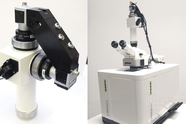
Figure 7. Computer-aided immunofluorescence microscopy system EUROPattern (EUROIMMUN Medizinische Labordiagnostika AG, Germany) for autoimmunity and infection diagnostics using Basler ace CMOS cameras for fluorescence imaging. Courtesy of Basler AG.
Point-of-care systems are increasingly gaining significance in medical diagnostics. Among other things, they make it possible to establish better medical care even in economically and infrastructurally weak regions, thanks to simple and inexpensive applications. Lab-on-a-chip technologies enable the processing of patient samples on a small chip, without requiring complex lab equipment.
Fluorescence applications can also be found in the practice of medicine. In surgical microscopy, for example, the operating doctor is increasingly supported by specific fluorescence markings of blood vessels or tumor tissues, allowing the doctor to operate with perfect precision using FGS (fluorescence-guided surgery). Dentists can also offer faster and more specific treatment, such as making tooth areas affected by decay selectively visible during the treatment. Last but not least, fluorescence-microscope applications are used in pathology to examine tissues from patient biopsies for possible diseases.
The life sciences offer a broad range of fluorescence-based applications in which microscopic examinations have a significant share. Immunofluorescence microscopy enables specific detection of particular proteins — for example, to detect or clarify their localization in cells and tissues or as markers for beginning cell death, depending on particular test conditions (Figure 8). Nowadays, live cell imaging can also be performed for longer time periods on automatic systems.
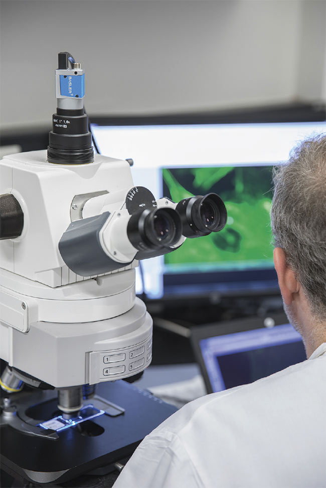
Figure 8. A manual immunofluorescence microscope with a Basler MED ace camera. Courtesy of Basler AG.
Miniaturization and parallelization to increase analysis numbers are especially significant in pharmaceutical research, since a very high number of samples are screened analytically in the search for new active substances. This is where microarrays and high-content screening systems are used (Figure 9). With automatic colony counters, fluorescence markers can be used in petri dishes to select successfully transfected cells to subsequently pick a sample of the respective colony. This means it is verified whether particular genetic material was actually transferred to the cell as part of an experiment, and the researchers can continue using this for their research.
Aside from the life sciences, fluorescence-based methods are also used in other areas, such as material analysis and forensics.
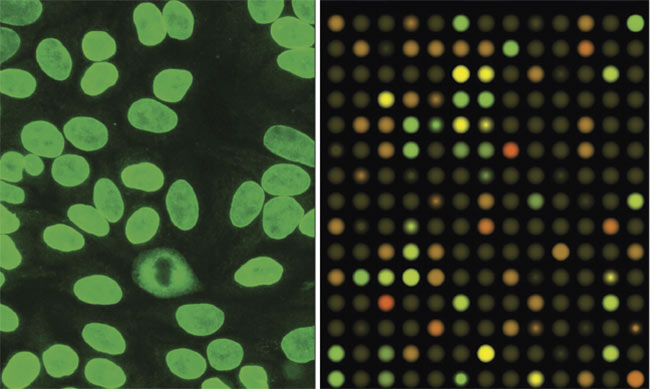
Figure 9. Immunofluorescence microscopic assay in autoimmune diagnostics (left). A DNA micro-
array used in cancer and other disease research (right). Courtesy of Basler AG.
/Buyers_Guide/Basler_AG/c1527
Published: September 2019
Glossary
- fluorescence
- Fluorescence is a type of luminescence, which is the emission of light by a substance that has absorbed light or other electromagnetic radiation. Specifically, fluorescence involves the absorption of light at one wavelength and the subsequent re-emission of light at a longer wavelength. The emitted light occurs almost instantaneously and ceases when the excitation light source is removed.
Key characteristics of fluorescence include:
Excitation and emission wavelengths: Fluorescent materials...
- fluorescence microscopy
- Fluorescence microscopy is a specialized optical imaging technique used in biology, chemistry, and materials science to visualize and study specimens that exhibit fluorescence. Fluorescence is the phenomenon where a substance absorbs light at one wavelength and emits light at a longer wavelength. In fluorescence microscopy, fluorescent dyes or proteins are used to label specific structures or molecules within a sample.
The basic principles of fluorescence microscopy involve illuminating the...
Featuresfluorescencefluorescence microscopyImagingSensors & DetectorscamerasCCDCMOSsCMOSBSIBiophotonics