Camera-based systems for defect detection reduce production costs and improve quality.
Dave Jenkins, Radiant Imaging Inc.
Popularity has its drawbacks, which for the increasingly popular flat panel display industry means that both production efficiency and quality control must be maintained. The two are not always synonymous, however. Ensuring quality requires reliable inspection of individual components or assemblies at many points throughout the production process.
Human visual inspection still plays a part, but it can create problems throughout the display supply chain. It slows production, and its subjective nature can lead to disagreements between supplier and customer over product quality at the component level. Rejected parts, which must be scrapped or reworked, negatively affect the economics of producing flat panel displays.
Traditional machine vision systems supplement visual inspection in display manufacturing, but they are not without their own set of problems. Over the past few years, camera systems have been developed specifically to meet the needs of flat panel display metrology. These systems are calibrated in such a way that the results can be combined with human visual inspection to provide an objective, operator-independent measure of display defects.
The purpose of a display system is to provide a stimulus for human visual perception, to communicate information in terms of language and images. In this context, a display defect can be defined as something that inhibits or impairs the effective communication of this visual information.
Many types of defects can occur in displays, including large- and small-scale variations in output brightness (luminance) and color (chrominance). Collectively, these are classified as pixel or Mura defects, the latter of which is derived from a Japanese term meaning nonuniformity or blemish. Displays also can contain cosmetic surface defects such as scratches.
Display defects
Mura defects can arise at several points in the production process, depending upon the display technology involved. For example, liquid crystal displays (LCDs) usually consist of a backlight, a diffuser, a liquid crystal panel, polarizers and brightness-enhancement film. Small-scale defects in backlights are usually caused by particulate contamination and dust (Figure 1). Larger defects might arise from fingerprints or gross variations in the backlight construction materials. All create nonuniformities in the delivered illumination.

Figure 1. This image of a liquid crystal display thin-film transistor backlight was processed to show both large- and small-scale variations in color and brightness.
Diffusers also may have similar problems with particulates. In addition, the injection-molding process commonly used to fabricate diffusers can lead to stress patterns in the material, creating birefringence. This can translate into a variation in brightness or color in the final display (Figure 2).
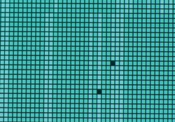
Figure 2. Processed image of a monochrome organic LED display shows dead pixels and color and brightness variations.
Polarizers may contain pinholes and dust, or may have surface defects (scratches, ripples, bumps) caused by the rolling process. The latter is also true of brightness-enhancement films, which are similarly produced.
Typically, the liquid crystal panels themselves are not a major source of display defects because they are subjected to rigorous yield management solutions, and their electrical and optical characteristics are directly tested and assessed. Defects also can be introduced during the assembly process by factors such as component misalignment and mechanically induced stress.
For most display manufacturers, many of the components are supplied by outside vendors. Because the final display can be affected by problems in any one of these components, it is vitally important for everyone within the supply chain to work with a common set of standards and definitions as to what constitutes a defect (Figure 3).
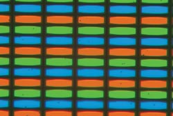
Figure 3. Under magnification, subpixel defects in a color organic LED become visible.
The traditional approach to detecting defects throughout most of the display industry is human visual inspection, which may be adequate for small displays manufactured in limited quantities. In this case, operators have the time to examine each production unit individually. Also, the products are physically small enough to allow the operator to manually manipulate them to optimize the viewing angle, as well as to readily reach all parts of the surface for examination with a magnifier.
The metrology challenge
However, this approach isn’t viable for large flat panel displays, such as plasma and thin-film transistor LCD televisions, which are typically laid flat as they move down the production line. Because they’re too heavy to be lifted easily, it is more difficult for an operator to rapidly change the viewing angle or to observe the entire display area, especially under magnification.
Human inspection also presents problems for high-volume manufacturing environments. Individual operator fatigue and operator-to-operator inconsistency can affect the quality and conformity of results. Furthermore, human inspection can slow production, which has a significant cost impact.
Using instrumentation for detecting defects can speed up production and reduce subjectivity, and there is no reason why metrology equipment should not be capable of identifying small defects. This is important, because it’s the little defects that can cause disagreement between the vendor and the customer over whether a “minor” flaw is acceptable or not. Developing objective criteria for Mura defects based on instrumentation financially benefits everyone along the supply chain. It minimizes returned parts and reduces the time and costs associated with those supplier/consumer disputes. It also enables component manufacturers to focus their process- and quality-control efforts on the factors that result in a tangible defect. Ultimately, this will improve production yields.
However, keep in mind that the ultimate measure of display performance is the way it looks to the human eye. For this reason, it is neither possible nor desirable to completely remove the human element from the testing/production process. The essential challenge in creating useful metrology systems for display defects is to develop instrumentation that successfully correlates with human visual inspection.
Calibrated hardware
Radiant Imaging Inc. of Duvall, Wash., has approached this problem by breaking it down into two segments. The first is based on calibrated, CCD-based imaging systems that can make absolute, repeatable measurements of display luminance and chrominance. The second uses software that can detect, classify and measure defects imaged by the first.
This methodology avoids the well-recognized limitations of traditional machine vision systems, which typically make only relative, analog measurements and don’t have sufficient dynamic range or signal-to-noise characteristics to consistently identify subtle color and brightness defects. Furthermore, they cannot quantitatively measure brightness and color as observed by the human eye. That is, they are not calibrated to measure true luminance or chrominance.
These are all problems, because image-processing algorithms can’t deliver consistent results unless they are supplied with data that has both absolute accuracy and repeatability. In other words, it’s essential that the camera system respond the same way each time to a given input. Otherwise, it’s impossible for the software to make a proper correlation with human visual response.
A critical key to achieving absolute accuracy and repeatability is to calibrate the data-acquisition hardware using a technique called flat fielding, which removes all camera-dependent factors from the acquired data. Even the best CCD cameras exhibit some nonuniformities in their pixel response, but flat fielding produces images that show only features derived from the device under test. In addition, dust particles on the CCD, lens and filters, as well as scratches and other imperfections in the optics, may result in local variations in camera response.
Flat fielding is accomplished by having the camera image an evenly illuminated source, such as an integrating sphere. The response to this input is applied to images of the device being tested. Separate flat-field corrections must be applied for each configuration of optics and filters that is used. Besides flat fielding, Radiant Imaging has found it necessary to use a number of other calibration techniques to eliminate spurious effects such as stray light.
Another critical step in system calibration is matching results to a specific color space to correlate with the human visual experience of colored light; we typically use the CIE color space. The details of color calibration are complex, but employing multicolor calibration techniques has been successful.
Essentially, results from the system are compared with those from a spectroradiometer at several points, and nonlinear correction algorithms are applied so that the system delivers correct results over its entire color gamut.
Once calibrated, the system response must remain constant over time. One aspect of this stabilization is to control the temperature of the CCD, which holds detector response to a given input constant. Cooling a CCD reduces the signal-to-noise ratio, enhancing the quality of the data.
In real production applications, multiple images may be required to detect small defects, especially at the subpixel level. This can be accomplished by moving a single camera and taking several sequential images, or with a system consisting of multiple cameras that capture images simultaneously. Also, using external illumination — possibly from a variety of angles — is often necessary to show surface defects such as scratches.
Once high-quality data has been acquired by the camera system, the next step is to interpret it. The goal is to accomplish this by using methods that correlate well with human visual perception. For well-defined, high-contrast defects (essentially blobs), this is fairly straightforward. The system can be set to look for certain levels of contrast in both brightness and color, and to indicate these as a display defect. The detection thresholds also can be related to feature size, because an average user is more likely to discover a larger defect than a smaller one of a given contrast.
However, the human visual system is sensitive to much more than just localized, well-defined defects. Repetitive patterns such as subtle stripes can be distracting. The effect on the viewer is dependent upon pattern contrast ratio and spatial frequency. The effects of certain types of features can be exaggerated by the human perceptual system. If the camera is supplying adequate, low-noise data, this information can be extracted from the image (even more effectively than the eye alone can). Then various pattern-recognition and image-processing algorithms can be used to identify those features that would be perceived as bothersome by a human viewer (Figure 4).

Figure 4. The human visual system sometimes sees things that aren’t there, such as the illusory blue square between the circles. Image-processing algorithms must duplicate some of these perceptual artifacts.
Although the preferred method of image analysis is one based on thresholds, the technique may not be able to identify all defects. Statistical approaches that compare each sample under test to a statistical norm may be applied. Learning algorithms such as software neural nets are also used to mimic human visual response.
It’s important to realize that each inspection task is an individual case, and a single set of hardware and software tools cannot be expected to work for all customers and all technologies. Camera and illumination hardware must be optimized for the particular inspection task and environment. Software algorithms must be designed and optimized to look for the particular defects that might occur and that are of concern for that specific product type, and to perform this function under the particular illumination and testing conditions that prevail.
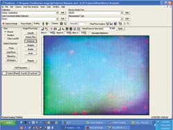
Figure 5. Image processing of a projection display reveals a number of small color and brightness defects as well as a “stuck image” of a checkerboard pattern that the projector had displayed a few minutes before.
Despite the fact that the annual worldwide market for flat panel displays is approximately $50 billion and growing, the display industry is still in its infancy in terms of production metrology. The use of instrumentation to supplement human inspection on the production line promises to improve display quality and manufacturing yields and, ultimately, to reduce costs.
Meet the author
Dave Jenkins is vice president of sales and marketing at Radiant Imaging Inc. in Duvall, Wash.