Pulses of 100 fs or less can perform micromachining tasks not achievable by any other laser process.
Marco Arrigoni, Coherent Inc.
The drive for miniaturization in electronics, photonics and biomedical devices is spurring an ever-growing need for laser micromachining. Femtosecond laser pulses provide unique capabilities for producing features as small as a few tens of nanometers and for creating microscopic holes, cuts and structures within transparent materials.
Laser micromachining must meet two important goals. First, it must be able to create extremely small features and, second, this must be accomplished with minimal peripheral thermal damage and associated debris. The traditional approach to achieving these ends has been to use short-wavelength (UV) lasers, which fill both of these requirements.
UV micromachining
Short wavelengths enable small feature sizes because the focused spot size is limited by diffraction, which scales linearly with the laser wavelength. In traditional micromachining applications, the minimum feature size is usually about half the size of the laser wavelength used. Thus, a 266-nm laser enables the production of features that measure about 150 nm.
In addition, UV micromachining minimizes peripheral damage because it is accomplished through a process called ablation. In this approach, high-energy UV photons directly excite electrons in the target material, breaking the bonds that hold the atoms together. Ablation produces virtually no bulk heating or splattered material. In contrast, longer-wavelength lasers with their lower-energy photons simply heat material until it is boiled off.
Unfortunately, UV laser micromachining can’t be readily extended below about 157 nm because of a lack of both lasers and transmissive lens materials for shorter wavelengths. To move beyond this barrier and enter the realm of nanotechnology, the process of ultrafast laser micromachining is being developed. This approach utilizes an ultrafast laser to drive multiphoton absorption. Specifically, when a mode-locked laser beam is focused to a small spot size, the high intensity at the focal spot causes the electrons to be excited by simultaneous absorption of multiple low-energy photons. Material is ejected as atoms or small molecular fragments.
Multiphoton absorption
As with UV micromachining, processing with multiphoton absorption produces almost no peripheral heating. But, even more important, multiphoton excitation, using Ti:sapphire lasers with output centered at 850 nm has already demonstrated the ability to produce features as small as 70 nm. This is possible because of the nonlinear power dependence of multiphoton excitation, compared with the conventional (one photon) absorption of laser light.
With linear absorption, the laser processing power scales linearly with the incident laser power, to a first approximation. But with multiphoton absorption, the processing power scales as (laser power)N where N is the number of photons simultaneously absorbed. N typically ranges from 3 to 10, depending on the peak power of the laser pulse and the material being processed. This high-order dependence on laser intensity means that the effective processing profile of the laser beam can be much narrower than its Gaussian intensity profile (Figure 1).
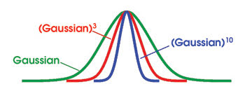
Figure 1. In multiphoton absorption, the processing power depends on (laser intensity) N, where N is the number of photons simultaneously absorbed. Because of this nonlinear dependence on laser intensity, the effective processing profile of the beam is much narrower than the Gaussian intensity profile.
Another important benefit of ultrafast laser ablation is that it can be used to machine “transparent” materials — high-bandgap materials that cannot be machined using Q-switched UV lasers. Even if the material has only a minute absorption coefficient at the laser wavelength, the high laser intensity at the beam focal waist will efficiently drive the nonlinear multiphoton absorption process. Thus, near-infrared ultrafast lasers can micromachine a very wide range of materials, including metals, plastics, glass and ceramics.
Furthermore, femtosecond laser pulses can be used to machine inside these transparent substrates without affecting the surface or outer layers. This three-dimensional control is possible because the laser energy is absorbed only at the beam waist; with small pulse energies and high-numerical-aperture optics, the laser intensity exceeds the ablation threshold only over a small axial distance Z (Figure 2). Axial resolution is maximized as the ratio of pulse width to pulse energy is reduced. Only femtosecond lasers (as opposed to picosecond lasers) can deliver submicron Z-axis resolution. Increasing the pulse energy of a picosecond laser to minimize the pulse width/pulse energy ratio is not an option; the higher pulse energy means that the ablation threshold will be exceeded over a broader X-Y-Z range.
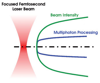
Figure 2. When a femtosecond laser is focused with high-numerical-aperture optics, the beam intensity only exceeds the multiphoton ablation threshold over a short Z distance.
Among the types of femtosecond lasers currently on the market are oscillators, high-repetition-rate amplifiers and high-pulse-energy amplifiers. In a mode-locked, femtosecond laser system, there is a trade-off between pulse energy and repetition rate. In a typical Ti:sapphire oscillator, they are 10 to 30 nJ and 76 MHz, respectively. Although 30 nJ might seem minuscule in the context of materials processing, with a pulse duration of 100 fs, this translates into an impressive peak power of 300 kW.
This type of laser oscillator can be used to seed amplifiers with either a high repetition rate or a high pulse energy. For example, the Coherent RegA amplifier delivers as much as 250 kHz and 6 to 8 μJ. The company’s Legend is a typical high-energy amplifier with up to 5 kHz and 2.5 mJ. Each type of ultrafast laser will have its own niche of applications, but we believe that high-repetition-rate femtosecond devices will ultimately secure the largest market share.
There are two reasons for this. First, these lasers offer a unique operating domain with respect to other nonultrafast devices. And second, this operating domain matches the requirements of two- and three-dimensional submicron machining in the field of nanotechnology, in terms of both energy per pulse required to produce nanoscale features and the repetition rates required to achieve economically sensible throughputs.
Emerging applications
K. Venkatakrishnan, a senior R&D engineer at Xsil Ltd. in Dublin, Ireland, a supplier of integrated workstations, said, “Although we are still in the early days of ultrafast applications, it is already clear that high-repetition-rate femtosecond lasers will be one of the winning technologies.” He cited several applications to support this contention, including semiconductor mask fabrication and repair, where the goal is to ablate small chads of material that have been left by the mask-generation process.
“Spatial resolution, process control and throughput are key considerations,” he said. “The traditional technology is FIB — focused ion beam — but this is a slow process. The high-repetition-rate femtosecond amplifier has proved it can do the job faster and for a lower cost than FIB. We originally tried a picosecond laser, but we could not achieve the necessary spatial resolution.”
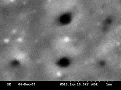
Figure 3. With femtosecond pulses, holes smaller than the diffraction limit can be created because of the nonlinear dependence on laser intensity. As shown in this silicon sample, even smaller holes can be drilled by adjusting the pulse energy so that only the center of the beam exceeds the ablation threshold. Courtesy of Xsil Ltd.
He added that Xsil has demonstrated X-Y resolution of λ/20 of the laser spot diameter — producing holes with diameters as small as a few tens of microns (Figure 3). “The reason for this high reduction factor is the short pulse duration. For a given pulse energy, the multiphoton absorption is extremely efficient and confined to the very center of the laser spot, where the intensity exceeds the ablation threshold. Moreover, we can further enhance the spatial resolution by lowering the pulse energy to reduce the area of the laser spot where the intensity exceeds the multiphoton ablation threshold. But with pulses longer than about 100 fs, we just can’t approach this high spatial resolution.”
Drilling tiny (2-μm diameter) holes in contact lenses is another potential application. The limiting factor that determines wear time is the fact that the lenses prevent oxygen from reaching the front surface of the cornea. In a study carried out at Pen Centre, Nanyang Technological University, in collaboration with Igel CM Laboratory (a manufacturer of contact lenses), both in Singapore, Venkatakrishnan explored drilling holes through the lenses to address this problem. These holes have to be large enough to permit air diffusion, but small enough that they don’t interfere with vision. “This is an application that simply cannot tolerate recast debris around the hole, or eye irritation will result from the rough lens surface. Even picosecond lasers produce too much debris for this purpose, but we found that femtosecond laser pulses can do this job quite nicely,” he said.
As with others in the field, Venkatakrishnan sees nanotechnology driving a new market for high-repetition-rate femtosecond pulses. He said, “Femtosecond will be preferred over picosecond for its higher X-Y resolution, but let’s not forget about Z-axis resolution. Many applications, such as ablating a thin layer without damaging underlying layers, or creating three-dimensional structures, need close control over this parameter [Figure 4]. These applications will use pulse energies of less than 20 μJ to ablate a few tens of nanometers per pulse. And this goes hand in hand with the need for a high pulse repetition rate to deliver economically enabling throughput rates.
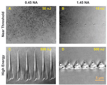
Figure 4. These side-view images of holes created in glass show how the three-dimensional resolution is dependent on both pulse energy and beam focusing. Courtesy of Eric Mazur.
“To summarize, the use of femtosecond pulses with low pulse energy makes the process deterministic and very controllable, by removing the statistical element associated with high pulse energies and longer pulse durations.”
Eric Mazur of Harvard University’s physics department is a pioneer in the use of lasers in nanotechnology to machine on the surface of, and within, transparent media. His group has used microjoule femtosecond pulses to produce miniaturized photonic components, such as Bragg gratings, Mach-Zehnder interferometers, 3-D beamsplitters, complex waveguides and monolithic amplifiers. He remarked that the ability to create these 3-D structures within transparent substrates enables the production of novel device architectures, as well as closely stacked functionality.
Unlike open processing, such as hole drilling, creating these structures often requires closed processing, where there is no way for the energy to escape from within the material. This process can really benefit from the high-repetition-rate amplifier. “In many of these components, we use the laser to transform the material; e.g., to a different refractive index,” Mazur said. “Here we rely on low-energy femtosecond pulses to give us high spatial resolution deep within the transparent substrate. But because there’s no place for released energy to escape, the high pulse repetition rate causes an energy accumulation leading to localized melting. The resolidified material then has a different index — defining a waveguide, for example.”
Microfluidics is another area that looks promising for femtosecond lasers. This refers specifically to chemistry experiments where picoliters of reagents are mixed, reacted and optically probed in 3-D glass and plastic substrates. Here the laser can be used to form waveguides to allow efficient probing of fluorescence or absorption properties as well as to create the flow tubes and channels by reverse drilling (Figure 5).
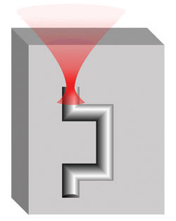
Figure 5. The ability to machine inside transparent substrates means that elaborate shapes and convoluted holes can be created.
In conclusion, high-repetition-rate femtosecond lasers define a unique operating niche in nanotechnology that cannot be filled by any other type of laser. The need for this type of processing is steadily increasing in a wide variety of application areas. Laser manufacturers are meeting this need with more mature and reliable ultrafast products, such as “one-box” Ti:sapphire lasers and laser amplifiers. These will ensure market growth and the long-term success of a technology that has been used almost exclusively by the research community for many years.
Meet the author
Marco Arrigoni is director of marketing for Coherent Inc.’s Advanced Systems Business Unit in Santa Clara, Calif.