Innovations in the use of 13.5-nm light set the stage for volume introduction of 7- and 5-nm nodes.
IGOR FOMENKOV, STEPHEN HSU, AND RODERIK VAN ES, ASML HOLDING NV
For years, 193-nm immersion lithography enabled foundries to create increasingly smaller features on silicon wafers. The technique involved shining 193-nm light through a patterned surface that cast a pattern onto a blank silicon wafer. But problems arose: At 193 nm, the light is much longer than the size of the features, requiring the use of a number of different photomasks and numerous passes to create the finished pattern.
That has led the semiconductor manufacturing industry to investigate the use of 13.5-nm light in the portion of the spectrum known as the extreme UV (EUV). At that wavelength, the light source is much closer in size to the final features, thereby eliminating a number of the steps required in traditional lithography setups.
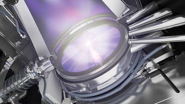
The extreme UV (EUV) source vessel is where a powerful laser hits tin droplets to generate EUV light. The light is focused by the collector mirror at the bottom. Courtesy of ASML Holding NV.
With the 10-nm node in commercial production, the semiconductor industry is getting ready for lithography for 7- and 5-nm nodes. Besides being a significant scaling step, these devices will likely see the introduction of EUV technology to ensure cost-effective manufacturing. Along with the cost benefits, process developers also target improvements in shrink, logic density, and process complexity.
Since a leading-edge multiple-patterning process requires up to twice as many total lithography exposures using argon fluoride immersion (ArFi) systems, it takes longer to develop and has smaller margins of error. An EUV-based process has advantages in terms of expected process complexity, yield, and time to market. Additionally, today’s EUV systems have already proved sufficient lithographic performance to meet imaging requirements for the most advanced nodes.
However, as EUV lithography matures over time, chipmakers will shift toward a deeper evaluation based on cost per layer to determine how many additional layers will move from multipatterning immersion to EUV. This will be affected by ongoing industrialization efforts to improve scanner throughput, availability, and stability to process many wafers in a short amount of time continuously.
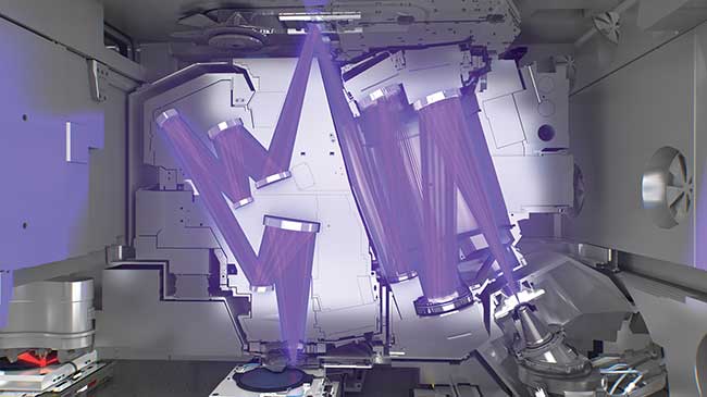
The full light path from EUV source to silicon wafer. The light is generated in the source (bottom right), sent into the illuminator (mid right), which controls the light beam, and reflects off the mask with the chip pattern (top) before being focused in the projection optics (mid left) and exposing the wafer (mid bottom). Courtesy of ASML Holding NV.
Introducing this completely new lithography technology will be a significant transition for the semiconductor industry. Substantial progress has been made in recent years to ensure its adoption and extend Moore’s law.
Performance parameters
Following years of development and testing, EUV systems have reached levels of productivity that give chipmakers the confidence to place orders. Several such systems have shipped and are operational, showing stable imaging, overlay, and focus performance.
One such system developed by ASML Holding NV uses dense lines and spaces at half-pitch of 13 nm (pitch 26 nm), and isolated spaces of 16 nm at pitch 112 nm, to match the 5-nm node imaging requirements.
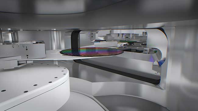
The wafer handler is a mechatronic module that moves wafers in and out of the (vacuum) heart of the system. Shown is a wafer being taken into the vacuum environment, where it will be measured and exposed. Courtesy of ASML Holding NV.
A full-size pellicle has successfully been manufactured without defects that influence the imaging. Throughout 2017, significant progress was made to reduce the intrinsic pellicle defectivity level to zero, while enabling productivity performance (power, lifetime, and transmission).
Productivity of 125 wafers per hour (wph) has also been demonstrated, a closely watched metric of the economic value of EUV, since higher throughput means that one system can produce more chips. In 2006, the very first EUV prototype system needed more than 21 hours to expose a full wafer. At 125 wph, today’s EUV systems run more than 2600 times faster.
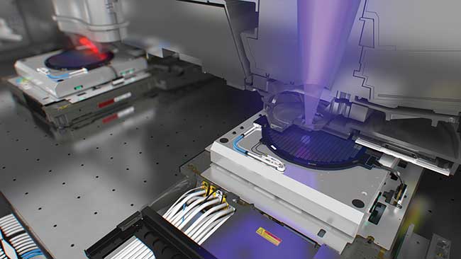
This ASML lithography system supports EUV volume production at the 7- and 5-nm nodes. Courtesy of ASML Holding NV.
System wafer throughput is dependent on several parameters, including the amount of power the EUV light source can generate, higher optical transmission, and reduced scanner overhead. This is because an exposure must happen with a certain amount of energy — the dose.The more EUV photons are available for exposure, the faster this dose can be delivered to the wafer and thus the higher throughput. Process control in lithography relies on the ability to control the energy delivered to the wafer to expose the resist. EUV photons intrinsically have a higher energy, requiring advanced dose-control algorithms to enable the specification for critical features. For critical features, the exposure latitude is on the order of only a few percent.
Scaling EUV power to 250 W
Among the main advancements that enabled higher throughput is a 250-W-capable light source, which delivers the energy needed for exposure to the wafer faster. Source power above 205 W is required to achieve 125 wph. The excess power could eventually be used to generate even higher throughput performance than 125 wph after stable performance is achieved.
EUV mirrors typically have a reflectivity of less than 70 percent at 13.5 nm, and there are about a dozen reflective surfaces, including the mask, which leads to very high power requirements for the EUV light source to overcome the high losses. To achieve a throughput of 100 wph at a typical scanner duty cycle of 60 percent, the power at the wafer should be greater than about 550 mW. This means the EUV source power provided to the exposure tool at intermediate focus should be greater than 200 W. For comparison, current 193-nm light sources for lithography have power levels of 90 W to support a throughput of 200 wph.
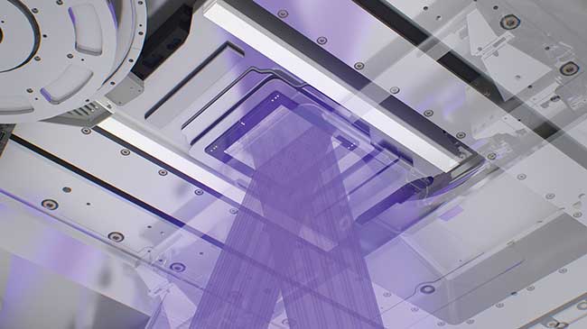
A reflecting mask (reticle) contains the blueprint of the chip pattern that will be exposed onto the silicon wafer. The EUV light, coming from the illuminator, is reflected off the reticle into the projection optics, which focus and shrink the pattern down. The reticle movement is fully synced with the wafer stage. Courtesy of ASML Holding NV.
The architecture of a high-power CO2 laser is of great importance for successfully scaling the EUV power emitted by the laser-produced plasma because it determines how the EUV-generated plasma is produced. When the architecture transitioned to seeded laser amplifier techniques, significantly higher conversion efficiency (CE) could be achieved, which resulted in higher EUV pulse energy and higher overall output power to the scanner. The technique involves a master oscillator, which generates a laser pulse that seeds the power amplifiers for single-pass gain extraction. The seed pulse is temporally triggered by the tin droplet such that the laser pulse and the tin droplet arrive at the primary focus at precisely the same instant.
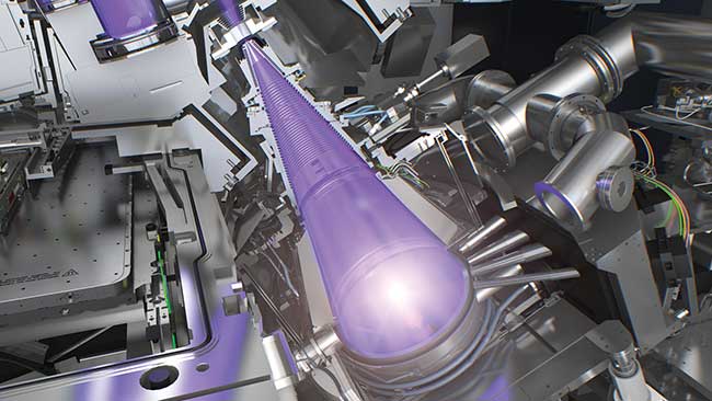
The vessel revealing the powerful laser hitting tin droplets to generate EUV. Courtesy of ASML Holding NV.
The prepulse is a laser pulse that hits the droplet prior to the main pulse, transforming the droplet into an improved target for enhanced plasma formation. The prepulse modifies the initial droplet into a larger target, resulting in increased surface area and more favorable density; this demonstrates the importance of precisely controlling the material distribution for better laser energy coupling. Prepulse technology has been validated as the path to higher-power output, and stabilized power of 250 W at intermediate focus has been demonstrated using advanced control technology to meet the dose stability target of <±0.5 percent 3σ with less overhead power needed to maintain the stability.
High-powered seed system
The development of a high-power seed system (HPSS) was initiated in 2015. The architecture has provided greater preamplification and improved isolation from parasitic effects. Because the HPSS has greater preamplification, it can more deeply saturate the power amplifiers, which has many benefits. One of these benefits is the increase in the peak instantaneous power of the laser pulse at the exit of the amplification chain, which has been shown to increase the conversion efficiency from laser pulse energy to EUV pulse energy. Therefore, not only does the HPSS enable the laser power to be increased, it also provides an increase in conversion efficiency, currently in excess of 6 percent on the most current configurations, or roughly 2 to 3× higher peak power than an NXE:3300 laser system.
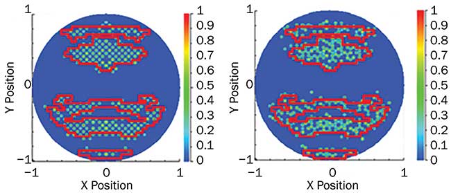
Use of the EUV light source allows for approximately 20 percent higher transmission or 10 percent higher throughput from NXE:3300 (left) to NXE:3400B (right). Courtesy of ASML Holding NV.
Such improvements in the main pulse characteristics, in addition to target formation developments, have enabled access to even more favorable plasma conditions. The development of higher-power CO2 lasers, together with higher CE achieved through improved laser-plasma energy coupling, and improved isolation, has resulted in an order-of-magnitude increase in EUV power at intermediate focus (IF) over the past few years.
The size and material distributions of formed targets using prepulse are also critical for CE and EUV power scaling. In addition to these parameters, target density (and its profile) and volume distribution of target material are critical for further improvement of CE and EUV power scaling. Coupling of the main pulse with an optimized target leads to higher CE, manageable debris, and improved EUV power scaling. An optimized tin (Sn) target has lower density than a liquid target, and when irradiated by the main drive laser pulse, a plasma without a steep density gradient is created.
More efficient use of target material and more efficient laser absorption are obtained by creating distributed laser absorption instead of localized laser absorption. More Sn ions are involved to emit EUV, leading to higher CE. With lower density targets, higher CE and EUV power were demonstrated. CE of 6 percent and 410-W in-burst EUV power at low duty cycle has been demonstrated on test sources in development laboratories.
Normal-incidence collector mirrors with >5 sr (steradians) light collection and high average reflectivity are being produced in volume and are showing increasingly long lifetimes in the field. Enhanced collector protection and in situ cleaning technologies are both expected to increase lifetime further.
Holistic control schemes
Additionally, given the increasing complexity in chip designs, materials, structures, and patterning techniques, it’s necessary to take a broader, holistic view of lithography. Chipmakers need a whole picture of how the intended design should and does print on a wafer, which requires computational, metrology, and control techniques to identify systematic defects.
The infrastructure is in place to meet the edge placement error (EPE) requirements by integrating scanner, process, and metrology performance in a cost-effective manner.
Inspecting critical defects on a chip or wafer is much like looking for a needle in a haystack — it helps to know the location and type of defects. Once you know the location, you can improve the process significantly faster.
Critical dimension scanning electron microscopy (CD-SEM) is the current process of record for CD metrology, with scatterometry metrology still under development. For isolated features, scatterometry metrology is already employed, since it is also used for the ArFi systems.
However, a high NA (numerical aperture) optical scatterometer can be used to densely measure in device CD and overlay errors. Large-field electron beam (e-beam) systems enable massive CD metrology, which can be used to characterize the local CD error. Local CD distribution needs to be characterized beyond 6σ and requires a high-throughput e-beam system.
By using a holistic patterning optimization approach, chipmakers can understand and minimize the EPE of the final pattern. EPE quantifies the pattern fidelity of a device structure made in a multipatterning scheme. Here, the pattern is the result of a sequence of lithography and etching steps. Consequently, the contour of the final pattern contains error sources of the different process steps. EPE is computed by combining optical and e-beam metrology data.
Optical metrology tools and computational models certainly offer improved process control, but an integrated e-beam metrology system further broadens the scope of control loops to include pattern fidelity.
By using advanced mathematical and analytical techniques, such as machine learning, new verification steps that compare where defects are expected to be and where they are found can help to continually check and calibrate the process models. Altogether, this holistic view results in a faster and more complete and accurate defect identification approach that enables chipmakers to inspect more wafers in the fab.
EUV into the next decade
Beyond 5 nm, with a 0.33 NA, double patterning is needed again. A high-NA EUV projection system is now being developed and will push the NA toward 0.55, enabling 3 nm and beyond to be printed with the same EUV wavelength using a single mask exposure.
Even as 0.33-NA EUV systems are being prepared to start volume manufacturing, development continues on a 0.55-NA EUV exposure tool. A lens design has been developed to prov
ide the resolution; this lens is paired with a flexible illuminator and more powerful source. Together with faster stages, this will provide high productivity at the anticipated large exposure doses. The more accurate stages, together with improved sensors, provide tight focus and overlay control, which is needed for future process nodes.
The promising progress in EUV lithography with high NA on the roadmap will help to advance Moore’s law in the coming decade.
Meet the authors
Igor Fomenkov, Ph.D., is an ASML fellow, conducting research and development of sources for extreme UV lithography. He holds over 100 patents. Fomenkov has a doctorate in physics and mathematics from the Moscow Institute of Physics and Technology (MPTI); email: [email protected].
Stephen Hsu is an ASML fellow, responsible for computational imaging product development. He holds 39 patents. Hsu is focused on sub-7-nm patterning technology development. He has a master’s in material science and engineering from the University of Utah; email: [email protected].
Roderik van Es is the director of product management at ASML, responsible for EUV’s next-generation 0.33-NA products. He has a master’s degree in applied physics from Delft University of Technology in the Netherlands; email: [email protected].
Acknowledgments
The authors wish to acknowledge the contributions of David Brandt and Jan van Schoot.