Scientists are learning more about the potential of excitons in applications from telecommunications to tunable lasers.
David W. Snoke, University of Pittsburgh
Electronics uses electrons. Photonics uses photons. Recently, the new field of spintronics has been defined, which uses spins for signals. Could we eventually have excitonics, circuits based on the control of excitons?
Although excitons have been investigated for more than 50 years, many people are still unfamiliar with them. An exciton is a quantum of excitation in a medium (Figure 1).
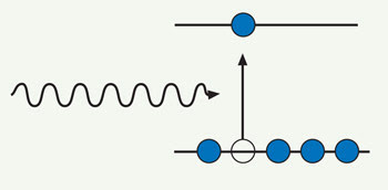
Figure 1. An exciton is an electron-hole pair that is created when an electron is excited from a lower- to a higher-energy state.
When a photon excites an electron from a lower state to a higher state, it leaves behind a positively charged hole. Essentially, two particles have been created for the price of one photon. The free electron and hole are not uncorrelated, however. Because the hole has a positive charge and the electron a negative one, there is a Coulomb attraction between them. If the attraction is strong enough, the two form a bound state — an exciton — analogous to the bound state of an electron and proton in atomic hydrogen. Excitons generally move freely through the medium, scattering from impurities and diffusing outward from the point of their creation.
The excited electron can fall back into the empty hole state, leading to the emission of a photon. Excitons, therefore, are metastable, with a finite lifetime known as the recombination lifetime.
Excitons transport energy and momentum, but not mass and charge. One way to think of them is as “renormalized photons” or as “photons dressed with mass.” While they exist, they interact with the medium like particles with mass, and electric fields and strain fields in the medium can manipulate them. At the end of the day, however, a photon has been absorbed at one place and emitted from another.
Excitons are ubiquitous in all types of matter, including semiconductors, metals and organic materials, in any system in which electrons can be excited to higher states. One reason why they are not better known is that materials with long exciton lifetimes are poor conductors, and the electronics industry thus has had little interest in such materials. Conversely, in systems with good conductivity and in many free charge carriers — for example, metals or heavily doped semiconductors — the Coulomb attraction between electrons and holes will be screened out, and excitons are unstable.
Semiconductors with a large dielectric constant have only weakly bound excitons, which can be observed only at cryogenic temperatures. In GaAs, the binding energy of excitons is 4 meV, so they ionize into uncorrelated electrons and holes at room temperature. By contrast, the exciton binding energy in some II-VI semiconductors can be 50 to 200 meV, so they are stable at room temperature. In organics, the binding energy can be up to 0.5 eV.
Excitons are more well-known in the world of optics and photonics, where they are the source of many nonlinear optical effects. The coupled electron-hole pair is strongly polarizable. Photonics researchers generally do not think about exciton transport or excitonic circuits, however. Because excitons in optical materials typically have very short recombination times — in the range of picoseconds to a few nanoseconds — they cannot move very far.
Controlling excitons
In the past 10 years, a method has been developed to control the lifetime and motion of excitons. Exciton lifetimes of up to tens of microseconds and motion over distances of up to a millimeter have been demonstrated.1 This opens up new possibilities of electro-optical interaction, in which optical signals are directly controlled by an electric field and are sent in circuits through chips in the same way as electrons.
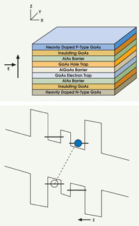
Figure 2. Indirect excitons with long lifetimes are created when an electric field is applied normal to two coupled quantum wells (top). The electrons move into one well and the holes into the other. Recombination occurs only if the electron and hole can tunnel through the barrier between the wells. The band structure of coupled quantum wells is illustrated (bottom).
The basic approach is illustrated in Figure 2. Two quantum wells are fabricated side by side, and an electric field is applied perpendicular to the wells. The electric field makes electrons and holes move into different wells. If there is a thin barrier between the wells, the carriers still will feel a strong enough Coulomb attraction to be bound into excitons, but the excitons will not be able to recombine unless an electron or hole tunnels through the barrier. The higher the electric field, the less likely that the carriers will tunnel and the longer the exciton lifetime will be.
Excitons of this type are called spatially indirect excitons, or simply indirect excitons. Because they have an intrinsic dipole moment resulting from the spatial separation, they are sometimes called dipole excitons. Early theoretical and experimental work on this system was done by researchers in Russia2 and at IBM’s T.J. Watson Research Center in Yorktown Heights, N.Y., and at Tokyo Research Laboratory.3 Recent experiments at the University of Pittsburgh and at Bell Labs in Murray Hill, N.J., have recorded lifetimes of more than 50 μs for indirect excitons in GaAs structures, consistent with theoretical calculations.
A key property of indirect excitons is that their energy shifts strongly with the local electric field. Figure 2, bottom, illustrates why: The energy difference between the electron and hole states depends directly on the drop in potential energy from one side of the well to the other. Known as the quantum-confined Stark effect, this leads to strong electro-optic and magneto-optic effects. Anything that shifts the local electric field will shift the spectral position of the indirect exciton transition; for example, small changes of magnetic field4,5 or of excitation power.6
Because the absorption or emission spectrum shifts strongly over tens of nanometers, coupled quantum wells have been proposed for optical shutters, detectors and tunable-wavelength lasers, but they have two drawbacks. For one, the oscillator strength of indirect exciton transition is low. (A long lifetime also corresponds to weak absorption.) For another, the time constant for switching is relatively slow by modern standards, with nanosecond time scales, because changing the electric field across the wells corresponds to charging a capacitor.
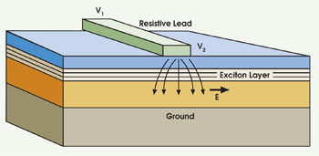
Figure 3. Excitons will follow a path in which the voltage across the wells varies from low to high.
The quantum-confined Stark effect also provides a way of putting a force on excitons to make them move in circuits. To make excitons move, one simply needs to create a gradient of the normal component of the electric field in the plane of the quantum wells. Because a high electric field corresponds to low energy for the indirect excitons, they will move toward the higher electric field. One way to do this is simply to send a current through a resistive top electrode (Figure 3). Excitons will follow the current path in reverse, from lower to higher voltage.
The total distance that excitons can travel depends on their lifetime, their average velocity and their scattering rate with defects and lattice vibrations. The diffusion distance l is given by

where D is the diffusion constant and t is the exciton lifetime. Typical values of D for excitons in coupled quantum wells at low temperature are 1 to 10 cm2/s, which implies diffusion distances of hundreds of microns.
Because they are aligned dipoles, indirect excitons repel each other. At a high density, therefore, pressure pushes the excitons to move faster and farther.
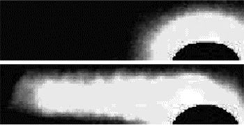
Figure 4. In the top image, no electric field is applied, and the excitons diffuse from the central region. (The dark circle on the bottom right is a disk approximately 50 μm in diameter that covers the region of laser excitation where the excitons are created.) In the bottom image, an applied electric field pulls the excitons toward the left.
Figure 4 shows images of indirect exciton motion in an applied electric field, in experiments7 performed recently by a group at Ludwig Maximilians Universität in Munich and at Universität Regensburg, both in Germany, that has demonstrated several methods for controlling excitons.8,9,10 Figure 5 shows similar drift of indirect excitons in experiments at the University of Pittsburgh using applied stress on the excitons.11 The stress reduces the bandgap of the material, making an energy minimum for the excitons at the point of highest stress.12
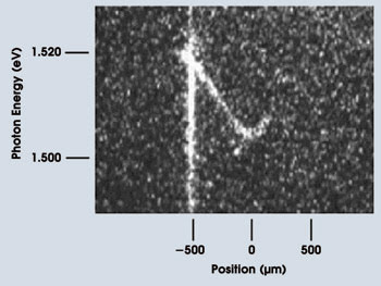
Figure 5. The point labeled 0 µm corresponds to a point of maximum stress and minimum bandgap. The excitons are created at 2500 μm at the point indicated by the vertical line (an artifact from the laser excitation). They then drift in the energy gradient toward the energy minimum.
Excitonic applications
What applications might excitonic circuits have?
One possibility is light collection — that is, the concentration of light energy from a wide area into a central point — to drive a chemical reaction or an electronic trigger. This is essentially the method that photosynthetic plants use to collect the energy of sunlight. Photons from the sun are converted into excitons in antennalike molecules and move toward a central collection point as a result of a gradient in the exciton energy.
Another is an optical delay line. Photons could be turned into indirect excitons, which would move slowly down a line until they were reconverted into photons at some region where the tunneling barrier between the electrons and holes had been removed. This motion of optical information is necessarily incoherent because the motion of the individual excitons is uncorrelated, although theorists have predicted the possibility of a superfluid exciton state that would preserve phase information.2,13,14 In such a case, the gas of excitons would be a Bose-Einstein condensate, analogous to the Bose-Einstein condensates of atoms in magneto-optical traps. Trapping the excitons in a harmonic potential, as in Figure 5, is the first step toward producing such a state.
The decrease in excitons’ energy as they move also means that excitonic circuits could be used as wavelength shifters. The amount of wavelength shift is easily controllable by the electric field. Moreover, the strong sensitivity of the exciton motion to the local electric field implies that their motion in circuits can be modulated in a transistorlike device.
Most of the present work on indirect excitons has been in GaAs-based structures. In these structures, excitons have a binding energy of only a few millielectron volts, which means that the experiments must be performed at cryogenic temperatures. There has been much promising work, however, on II-VI materials with deeply bound excitons, such as ZnTe and CdSe. In these materials, the binding energy of the excitons is 20 to 40 meV, so the excitons are stable even at room temperature, but the disorder in the present structures gives them a very low diffusion constant.
Much in modern electro-optics involves converting photons into uncorrelated electrons and holes that are pulled in opposite directions by an electric field. Excitonic circuits move electrons and holes in the same direction, enabling new possibilities in light collection and signal transmission.
Acknowledgment
The author gratefully acknowledges financial support from the US Department of Energy.
Meet the author
David W. Snoke is an associate professor of physics and astronomy at the University of Pittsburgh; e-mail: [email protected].
References
1. Z. Vörös et al (June 10, 2005). Long-distance diffusion of excitons in double quantum well structures. PHYS REV LETT, 226401.
2. Y. Lozovik and I. Yudson (Dec. 5, 1975). Feasibility of superfluidity of paired spatially separated electrons and holes; a new superconductivity mechanism. JETP LETT, pp. 274-276.
3. A. Alexandrou et al (Nov. 15, 1990). Electric-field effects on exciton lifetimes in symmetric coupled GaAs/Al0.3Ga0.7As double quantum wells. PHYS REV B, pp. 9225-9228.
4. V. Negoita, D.W. Snoke and K. Eberl (Jan. 25, 2000). Strong red shift of indirect exciton luminescence in low magnetic field. SOLID STATE COMMUN, pp. 437-441.
5. S. Denev et al (Nov. 15, 2002). Optical detection of magnetic fields using giant magnetoresistance in undoped coupled quantum wells. PHYS REV B, 205304.
6. V. Negoita, D.W. Snoke and K. Eberl (Jan. 15, 2000). Huge density-dependent blueshift of indirect excitons in biased coupled quantum wells. PHYS REV B, pp. 2779-2783.
7. A. Gärtner, D. Schuh and J.P. Kotthaus. Dynamics of long-living excitons in tunable potential landscapes. Available at http://arxiv.org/abs/condmat/0509142.
8. S. Zimmermann et al (July 13, 1998). Spatially resolved exciton trapping in a voltage-controlled lateral superlattice. APPL PHYS LETT, pp. 154-156.
9. S. Zimmermann et al (Nov. 15, 1997). Lateral superlattices as voltage-controlled traps for excitons. PHYS REV B, pp. 13414-13421.
10. C. Rocke et al (May 26, 1997). Acoustically driven storage of light in a quantum well. PHYS REV LETT, pp. 4099-4102.
11. D.W. Snoke et al (April 2005). Trapping long-lifetime excitons in a two-dimensional harmonic potential. SOLID STATE COMMUN, pp. 37-42.
12. V. Negoita, D.W. Snoke and K. Eberl (Oct. 4, 1999). Stretching quantum wells: A method for trapping free carriers in GaAs heterostructures. APPL PHYS LETT, pp. 2059-2061.
13. Y. Lozovik and O. Berman (May 1997). Phase transitions in a system of spatially separated electrons and holes. J EXP THEOR PHYS, pp. 1027-1035.
14. X. Zhu et al (Feb. 27, 1995). Exciton condensate in semiconductor quantum well structures. PHYS REV LETT, pp. 1633-1636.