Located in North-West Europe and bordering
the North Sea, Belgium and Germany, the Netherlands is well positioned as a key
trading center. It has excellent transport links, including Schiphol Airport in
Amsterdam, recognized as one of the major hubs in Europe, as well as the Port of
Rotterdam, Europe’s largest seaport.
It is little surprise then that it is home to many successful
photonics companies and attracts a global photonics presence.
The Netherlands’ approximately 200 photonics companies together
generate an annual turnover of about €5.5 billion ($7.7 billion). Two photonics
powerhouses that together contribute approximately 70 percent of this revenue are
electronics giant Philips of Amsterdam and lithography specialist ASML of Veldhoven.

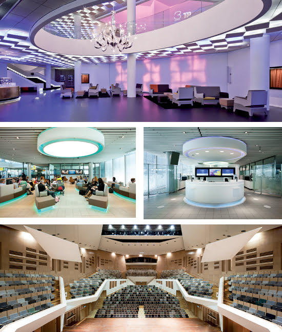
Top: In the foyer of the newly renovated Concert Hall Frits Philips
Eindhoven in the Netherlands, ceiling-mounted LEDs from Philips Design Consulting
provide illuminated pathways to guide people to the bar during the break. Bottom:
Inside the hall, Philips aims to influence people’s experiences through the
application of light, images and sound. Center: Schiphol Airport in Amsterdam showcases
the Innovative Gate, which was designed by Philips to provide air passengers with
a more pleasurable and relaxing experience. Top and bottom photos courtesy of Frank
Tielemans; center images courtesy of Intos Interior Contracting.
Traditionally, the strength of Dutch photonics has been in lighting,
driven primarily by Philips, and in manufacturing for high-end applications such
as semiconductor chips, which is largely dominated by ASML.
The Dutch government is keen to support growth in these areas,
and 2010 has seen the initiation of the second phase of a two-part road map for
its photonics industry.
The road map began in 2006 with the creation of the Innovation-Oriented
Research Programme Photonic Devices committee. Established with the support of the
Dutch ministry of economic affairs, the program was awarded a budget of more than
€20 million ($28 million) and tasked with bringing more focus and momentum
to Dutch photonics.
The ultimate aim is to rank Dutch research and companies right
up there with those of the seven leading countries in two key areas: advanced light
sources and detection systems, and the application of photonic devices in health
and medicine.
From 2006 to 2009, the focus was on developing advanced light
sources and detection systems. This year saw the start of a four-year program that
turned the country’s focus toward developing new photonic devices based on
generic technology, health care and medicine.
Another Dutch organization whose goal is to cultivate a healthy
industry is the Photonics Cluster Netherlands (PCN), which was initiated by the
Dutch Society for Photonics. Co-supported by TNO Science and Industry in Delft,
it will provide a platform for knowledge transfer in photonics for industry and
academia in the country.
“The PCN focuses on strengthening the network of photonics
companies and research groups, both within the Netherlands and abroad,” said
Bart Snijders, PCN chairman and business developer at TNO Science and Industry.
“The network activities are mainly targeted at increasing the economic activity
in the field of photonics.”
Philips enjoys a well-established culture of working closely with
research groups and industry. Although it has multiple sites throughout the world,
with sectors covering lighting, health care and consumer lifestyles, the technology
innovation is mainly concentrated in the Eindhoven region of the Netherlands.
Dutch concert hall gets an LED makeover
Three years ago, Wim Vringer, director of the Concert Hall Frits
Philips Eindhoven, imagined a new experience for concertgoers that involved light,
images and sound. Now, thanks to Philips Design Consulting, his vision has become
a reality.
“The Concert Hall Frits Philips Eindhoven is regarded by
some as one of the finest concert venues in Europe, mainly due to its excellent
acoustics,” said Menno Dieperink, art director at Philips Design. “There
was a feeling that the communal areas and exterior still had something of a provincial
feel. Vringer wanted to offer his public a world-class environment to match the
quality of the concert halls and of the performing artists.”
The results include illuminated pathways that use built-in ceiling
LEDs from Philips to subtly guide people to the bar during breaks; three Italian
chandeliers to add a touch of grandeur to the ambience; and a 13-m purpose-built
couch with integrated LEDs that illuminate a path between people as they sit in
various positions along its length.
Philips Design has an 85-year history in the Netherlands and abroad.
Jos Stuyfzand, director of the company’s Ambient Experience Design, said,
“The first Ambient Experience environments were in health care facilities,
where they help to ease patient anxiety, improve conditions for staff and boost
the external image of the hospital or clinic – an important consideration
in an ever-commercializing health care landscape. We now also implement Philips
Ambient Experience Design in other sectors, like hospitality and transport.”
An example of this can be found at the Innovative Gate at Schiphol
Airport, where Philips aims to provide a more pleasurable and relaxing experience
than your average departure gate offers with a combination of LEDs, multimedia and
physical restyling. The new gate also is said to help airlines speed up security
and check-in processes as well as to boost their brand image.
But with Philips repositioning itself toward health and well-being,
its lighting know-how is being applied in other domains, including minimally invasive
health care. A new field under investigation is the effect of light on organic cells,
which includes water purification, light-based therapy, the development of a light-based
epilator and growth aid for crops in warehouses.
Miniaturizing photonics boosts medical market
New developments in photonic components not only enables miniaturization
of optics-based medical devices, but also will reduce the overall price of such
devices, said Dr. Henricus J.C.M. “Dick” Sterenborg, a researcher at
Erasmus MC Center for Optical Diagnosis and Therapy in Rotterdam. Sterenborg is
co-founder of Luminostix, also of Rotterdam, which commercializes differential path
length spectroscopy – a technique developed at Erasmus.

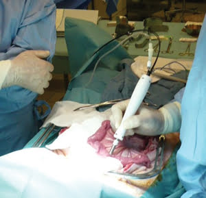
Optical measurements during bowel surgery are carried out to measure
the vascular properties in the surgical field. Courtesy of Luminostix b.v.
“As a consequence, optics-based medical devices will become
cheaper and can in the future be used in much broader fields of application, such
as the dentist’s office or in home care,” he said. “This will
enormously boost the market.”
Reflecting the trend to minimize is the Memphis Project (merging
electronics and micro- and nanophotonics in integrated systems), a consortium of
more than 20 Dutch companies and academic institutions that includes Philips, ASML,
Lionix, AMC Laser Centre and TNO.
The project aims to miniaturize and standardize optical technology
and to integrate with electronics. The hope is to open up new applications for the
use of light in medical diagnostics, health care, entertainment, telecommunications,
tracking and positioning.
Within this framework, the University of Twente in Enschede and
the Academic Medical Center, one of the largest hospitals in the Netherlands, are
working on developing a miniature optical coherence tomography device.
EUV forges a new era for chip makers
But it is not just size that is important. For lithography systems
maker ASML, smaller, faster and cheaper are at the top of the agenda. The company
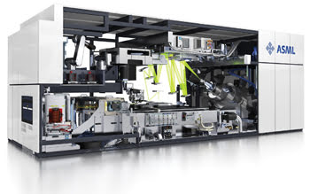
currently is shipping its new NXE:3100 lithography machine, which employs extreme-ultra-violet
(EUV) light to provide an imaging capability close to 20 nm.

ASML’s NXE:3100 extreme-UV lithography system. Courtesy of ASML.
Lithography machines have progressed from using UV light sources
with a wavelength of 365 nm to deep-UV sources of 248 and 193 nm, improving the
resolution at every step. EUV marks the next milestone in this progress and will
enable chip makers to reduce the size and increase the functionality of microchips
and consumer electronics equipment.
“Current lithography technology has been pushed further
than many would have thought possible even five years ago, but this has come at
the cost of increasing complexity and shrinking margins of error,” said Jojanneke
Strijbos, a corporate communications officer at ASML. “The industry has had
to reach deep into a bag of tricks to continue shrinking features sizes.
“With EUV, chip makers will be able to again expose a critical
layer in one single step – so no double patterning. EUV also has a credible
path from the initial 27-nm resolution to below 10 nm.”
Enticing students into optical careers
With so many high-tech companies in the country – including
small and medium enterprises (SMEs) such as Avantes, a spectroscopy and fiber optics
producer, and Genexis, a fiber-to-the-home equipment maker – the demand for
optical scientists and engineers is high.
Photonics companies typically recruit from one of three technical
universities in the Netherlands, each with a strong physics department: Delft University
of Technology, the University of Twente and Eindhoven University.
At Delft, a new focus on teaching classical optical design is
being introduced to better prepare students for their next step into industry.
“One of our new initiatives is to start a collaboration
between European research groups that are still active in optical design,”
said professor Paul Urbach, who heads up the Optics Research Group at Delft. “Classical
optical design is not taught in many universities anymore, but, nevertheless, it
is a very important subject for industry – in particular for SMEs.”
To attract students into optical studies, the group has set up
internships in industry from which students can select from a number of interesting
projects.
“For general applied physics students, it is true that they
often choose more fancy-sounding subjects, such as biophysics or quantum information,”
Urbach said. “To attract students, we try to bring across the message that
optics is actually very exciting and also very important for industry. Furthermore,
after graduating in optics, it is easy to get a job, and it is possible to stay
in the field because the demand for optical scientists and engineers is high.”
For Avantes’ technical director Benno Oderkerk it can be
a struggle to find staff with the necessary qualifications. “It is definitely
a problem to find photonics professionals. We have hired international professionals,
but also taken onboard technical engineers from other fields, such as mechanical
engineering and electrical engineering, and trained them in photonics ourselves.”
But, according to the Photonics Cluster Netherlands’ Snijders,
the photonics landscape could be set to change in the Netherlands with future
plans by some of the larger organizations to move to countries with lower salary
levels. That said, thanks to the significant expansion of SMEs, he expects the total
size of the photonics sector to stay at the current level.