
Diode Lasers Break into New Wavelengths, New Applications
New wavelengths, new production technologies and microassembly are all expected to help extend the reach of diode lasers in the future.
The field of diode lasers is a dynamic, fast-developing area, enabling new applications to emerge continuously. From pumping of solid-state lasers to materials processing and medical applications, the technology is broadening its appeal beyond the niche market to become a commodity product in several mainstream industries.
Diode lasers have long been utilized as a pump source for solid-state lasers, and they will continue to represent a very important part of this market, but manufacturers are confident that new avenues are opening up all of the time for these versatile and indispensable tools.
As the technology matures and the prices of laser systems drop (largely thanks to increasing output power per
device and simplifying packaging technology), the diode laser will become another instrument in the toolbox for several new industries, including automotive, medical and semiconductor, said Stefan Heinemann, a senior staff engineer at Trumpf Photonics, a part of the Ditzingen, Germany-based industrial laser company Trumpf.
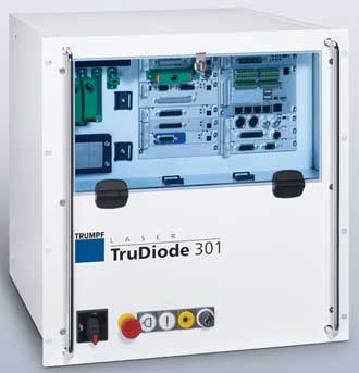
The TruDiode is based on small, compact diode modules interconnected by a fiber via wavelength coupling to achieve high output power. Photo courtesy of Trumpf.
“Laser brazing and welding is becoming more established in the automotive industry as a standard production tool, and it is expected to replace resistance spot welding,” Heinemann said. “The technology is especially important for aluminum welding, which gains more momentum as lightweight vehicles become increasingly important.”
Extending wavelengths
The wavelength of a diode laser depends on the bandgap of the semiconductor material used in the device. For example, diode lasers based on gallium arsenide (GaAs) and indium phosphide (InP) cover a large wavelength range; as Dr. Marion Lang, director of marketing at Toptica Photonics AG, has observed, the past 40 years have witnessed a tremendous upturn in the number of applications. These include the use of diode lasers in CD players (780 nm), DVD players (655 nm), telecom networks (1550 nm) and now Blu-ray players (405 nm).
Toptica Photonics AG of Munich – a manufacturer of lasers and systems for scientific and industrial applications – strengthened its diode laser portfolio last year by acquiring majority ownership of Berlin-based eagleyard Photonics GmbH.
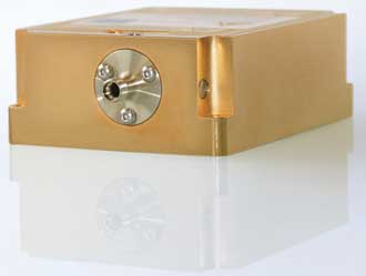
To expand its product portfolio, Jenoptik’s Lasers division increased the range of available wavelengths for its fiber-coupled medical laser modules to 1470 nm. Photo courtesy of Jenoptik.
Extending the wavelength range has inevitably led to an increase in the number of applications, including long-range sensing, IR countermeasures, welding of transparent materials (around 1.8 µm) and thin-film processing. The latter includes annealing of polysilicon, which is gaining momentum as the first systems with more
than 20 kW of power go online. Other thin-film processing involves the structuring of deposited films in consumer product manufacturing, including barcode writing or RFID (radio-frequency identification) tag manufacturing.
Advances toward shorter wavelengths are ongoing, with green diode lasers emitting around 530 nm now being reported.

Optical inspection of high-precision refractive micro-optical assemblies. Courtesy of LIMO.
Jenoptik Laser GmbH of Jena, Germany, sees growing markets in the medical sector, such as new therapies or improvement of established applications with new wavelengths. Procedures such as hair removal, vein removal and wrinkle reduction will continue to grow and gain market share. Fulfilling these demands for new wavelengths is a constant challenge for laser diode manufacturers.
Today’s laser-based hair removal, for example, is performed using quasi-continuous wave (QCW) stacks with an 808-nm wavelength. Jenoptik has recently developed an alternative operating at 760 nm, which not only is more efficient but also more comfortable for the patient.
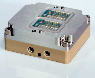
The double QCW stack from Jenoptik Laser GmbH is suitable for efficient and more comfortable hair removal, and also for pumping applications and materials processing. Photo courtesy of Jenoptik.
Also new at Jenoptik is the double QCW stack, which is suitable for hair removal and pumping applications, as well as materials processing.
“As the size of the emitting area has been increased to approximately 25 × 12 sq mm with this stack, process speeds and, with it, productivity can now be increased significantly for the respective applications,” said Lars Wagner, product manager at Jenoptik. “The hermetically sealed housing is dustproof and gives the user a small, lightweight and robust design. In combination with the easy-to-handle service water cooling, the module can easily and quickly be integrated by the end user.”
For wavelengths that cannot be accessed directly, frequency-converted systems (frequency-doubled, frequency-quadrupled) are available. For example, newly developed tapered semiconductor amplifiers have further expanded the color spectrum of Toptica’s high-power, narrowband TA-SHG pro diode lasers. This tunable diode laser comprises a high-power semiconductor (TA) and an integrated frequency-doubling stage (SHG).
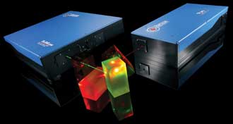
With newly developed tapered semiconductor amplifiers, Toptica’s amplified tunable diode laser systems (TA pro and TA-SHG pro) provide high power and more wavelengths. Photo courtesy of Toptica Photonics AG.
“Systems providing tunable, narrow-linewidth laser radiation around 556 nm (600 mW) and 606 nm (800 mW) are now available – e.g., for [ytterbium]-laser cooling and spectroscopy of rare-earth elements in solids,” Lang said. “The exclusive new TA chips enable a cost-effective laser system that outperforms Raman fiber systems with respect to tuning range (several nanometers) and narrow linewidths (well below 100 kHz).”
While they are expanding into shorter wavelengths, diode laser makers are also making inroads into the longer-wavelength regime. For example, high-power diode laser manufacturer LIMO Lissot-schenko Mikrooptik GmbH of Dortmund, Germany, develops and produces industrial laser systems for applications in the mid- to far-infrared (1470, 1550, 1940 and 2100 nm).
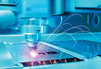
Energy-efficient laser fusion cutting of stainless steel. Photo courtesy of LIMO.
There is increasing demand for longer wavelengths for trace-gas spectroscopy (gases such as methane, carbon dioxide, carbon monoxide, oxygen, hydrochloride and water vapor), said Dr. Joachim Sacher, CEO of Sacher Lasertechnik, an external-cavity diode laser specialist based in Marburg, Germany. And for industrial applications and process control, markets are beginning to find use beyond telecom wavelengths (from 1630 nm up to 2.5 µm).
New materials and production technologies
Sacher has noticed great developments in the field of gallium nitride (GaN) materials, which enable devices operating at 520 nm. “We ourselves invest into GaSb [gallium antimony] development for offering high-level diode lasers greater than 2 µm,” he said.
Jenoptik’s GaAs diode lasers are capable of achieving wavelengths in the near-infrared region from 700 nm up to 1100 nm. And at Trumpf, material growth, device processing and packaging are optimized for reliable, high-power operation of devices with wavelengths from 900 to 1000 nm. Generally, the processing technology of growing GaN on sapphire has made significant progress, boosting yield and output power to more than 1 W from a 15-µm aperture for blue diode lasers emitting from 400 to 450 nm.
As part of a current European Commission project – iSense – that aims to transform laboratory instruments into portable, miniature devices that can be used outside the laboratory, Sacher Lasertechnik has developed the Micron Laser. The device is a fully tunable external-cavity diode laser the size of a thumbnail, which shrinks the conventional tunable diode laser system from its typical size of 20 × 8 × 8 cm.
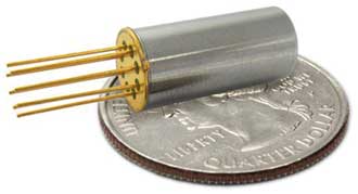
The Micron Laser from Sacher Lasertechnik is about the size of a thumbnail, compared with conventional tunable diode laser systems that can measure around 20 × 8 × 8 cm. Photo courtesy of Sacher Lasertechnik GmbH.
“Miniaturizing is a key step for bringing high-level laboratory laser technology into everyday applications in cars, medical handheld instruments, airborne, satellite applications, etc. We are just introducing this technology into the application-driven market,” Sacher said.
Similar developments are taking place with SHG systems in which small, innovative companies like AdvR Inc. of Bozeman, Mont., are developing SHG products on a module level. Sacher predicts that, within the next five years, this type of technology will replace the large-sized laboratory devices currently being sold.
Power for materials processing
The industrial materials-processing sector has long benefited from the use of diode lasers because of their unsurpassed efficiency in converting electrical power into laser light.
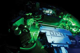
View into a frequency-converted system diode laser (TA-FHG pro). The laser light is efficiently frequency-converted in a resonant doubling stage. Photo courtesy of Toptica Photonics AG.
Some of the key challenges, according to LIMO’s Managing Director Dr. Paul Harten, are to design an optimized combination of laser beam shape, process gas flow and laser power to make direct diode lasers fully competitive with fiber, solid-state and CO2 lasers. Harten predicts that better beam quality at higher power levels in general will further broaden the application range of direct diode lasers, in particular when combined with flexible beam shaping.
But the holy grail for diode lasers must surely be to enter the largest market: laser cutting. This calls for not only a higher beam quality, but also an improvement in brightness and power, said Trumpf’s Heinemann.
“The first companies claim to reach performance levels (3 kW from 100 µm) with direct diode lasers, but the suppliers and users in industry need to validate the performance,” Heinemann said. “A continued decrease in price, an increase in performance and more user-friendly operation [are] needed to accelerate broad market penetration. The long-discussed $1/W must become reality.”
Jenoptik achieves high powers in the kilowatt region using a concept of coherent coupling of diode lasers. At SPIE Photonics West 2014 in San Francisco, Jenoptik’s Lasers & Material Processing division introduced a new generation of high-efficiency semiconductor lasers capable of achieving output powers up to 200 W in continuous-wave operation.
“With high efficiencies of over 70 percent and very low beam divergence, they combine high output and high brilliance with long lifetime and low cost,” Wagner said.
The company also introduced a further enhancement of its CN-mount heat sinks. Because of the double-sided cooling of the diode laser bars, this heat sink provides up to 30 percent higher cooling efficiency than the conventional mounting technology of diode laser bars.
“Through the further development of the manufacturing technique of the CN heat sink, it is possible to operate semiconductor lasers, mounted on it, also in a hard-pulse regime,” Wagner said.
“As a result of it, the use of these highly efficient passive heat sinks will be extended to many other fields of application like laser pumping and material processing.”
Published: September 2014