Manufacturing Matters
Paula M. Powell, Senior Editor
Buoyed by beam quality and system flexibility, diode-pumped lasers are continuing their
inroads into diverse micro- and macroworld applications.
They slice, they dice, they
weld. Diode-pumped solid-state lasers offer an ever-increasing degree of processing
flexibility and beam quality. These factors alone continue to strengthen their position
in industrial applications ranging from micromachining of silicon and even diamond
to conventional metal cutting and welding in flexible manufacturing environments
(Figure 1).

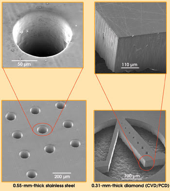
Figure 1. Nanosecond pulsing, high peak power and good beam quality are key to micromachining
hard-material workpieces with features in the 5- to 100-μm range and aspect
ratios up to 50:1. Courtesy of Lambda Physik.
Diode-pumped lasers are optically pumped crystal-based
devices, such as Nd:YAG and Nd:YLF, excited by a laser diode or an array of diodes
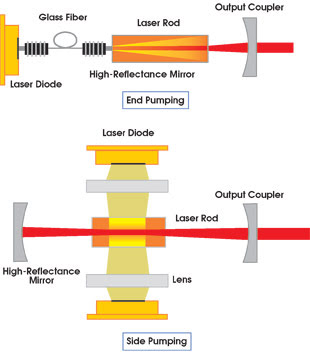
instead of a flashlamp or other intense light source. Systems can be either end-
or side-pumped, with rod geometries common and side-pumped slab designs beginning
to see more use in higher-power applications (Figure 2).
According to researchers at Bremen
Institute of Applied Beam Technology in Germany, advantages of diode pumping are
related to both cost and processing.1 They include power-consumption efficiencies
three or more times higher than that of lamp-pumped systems, as well as maintenance
intervals exceeding 10,000 to 20,000 hours instead of 500 to 1000 hours. Also key
is the higher beam quality, which the Bremen engineers say enables either a higher
power density at conventional focal lengths or a higher focal length at conventional
power densities.

Figure 2. End pumping (top) offers the benefit
of compactness. Side pumping (bottom) allows scalability of power
levels. Courtesy
of Rofin-Sinar.
Such lasers also are often designed
for second- or third-harmonic generation — 532 and 355 nm, respectively, for
a YAG lasing medium. One benefit seen by Werner Wiechmann, product manager at Lightwave
Electronics in Mountain View, Calif., is the capability to tailor processing characteristics
for specific work materials. Consider electronics processing applications where
lamp-pumped lasers could have problems with higher repetition rates. Diode-pumped
technology can offer lower repetition rates with higher-energy pulses or vice versa,
allowing one laser to handle both high-pulse-energy processing of copper and high-throughput
drilling of conventional dielectric materials.
Fiber optic beam delivery adds flexibility
by allowing end users to remove laser hardware from the processing line, either
to protect it from a harsh manufacturing environment or simply to conserve manufacturing
floor space.
So what’s the key to successful
processing? As with any laser application, end users must develop a fundamental
understanding of both the lasing mechanism and the manufacturing process.
Micromachining hard materials
Diode-pumped solid-state lasers have been the
workhorses of the electronics micromachining world for some time. Now researchers
at Lambda Physik USA in Fort Lauderdale, Fla., see them expanding into hard-part
processing. According to technology officer Sergei Govorkov, these applications
often have the following in common:
• Features in the 5- to 100-μm
range.
• The need to eliminate recast
material as well as microcracking.
• Aspect ratios of up to 50:1.
• Feature repeatability with
accuracy typically better than 1 μm.
• High processing speeds.
He explained that, when micromachining
hard materials with continuous-wave and long-pulse (>1 μs) lasers, such
as CO2 and free-running lamp-pumped solid-state lasers, high ablation rates can
come at the expense of feature size limitations. The culprits are often heat-affected
zone, microcracking or even poor beam penetration into the material. One reason
is that, as aspect ratios start to exceed 10:1, the laser beam undergoes attenuation
from multiple reflections off part walls. The beam also faces strong absorption
in the cloud of melt droplets and laser-generated plasma. “As a result,”
Govorkov said, “thicker materials require higher incident beam power, which
only promotes greater heat-affected zone and kerf width at the hole entrance.”
He and his colleagues believe that
diode-pumped solid-state lasers can successfully micromachine diverse materials
such as diamond, alumina ceramics, stainless steel and some carbon steels, using
a combination of very short pulses (15 ns or so) and high peak power (>0.2 MW).
During the ablation process, material escapes as vapor/plasma rather than as a liquid,
with the driving force for material ejection being extremely high pressure in the
vapor plume.
Moreover, per-pulse heat conduction
into the bulk of the material is limited. This, along with plasma shielding effects,
reduces thickness of the removed layer per pulse to just a few microns. As a result,
engineers can increase beam intensity for deeper penetration into the material without
damaging the surrounding material at the hole surface.
So far, the scientists have used short-pulse,
high-peak-power processing on materials as diverse as 0.47-mm-thick alumina ceramic,
0.31-mm-thick polycrystalline diamond and up to 1.0-mm-thick stainless steel. Their
test bed included a diode-pumped Nd:YAG laser that produced 15-ns-long pulses at
a 10-kHz repetition rate, with average power reaching 30 W at 1064 nm, 15 W at 532
nm and 10 W at 355 nm. The laser had a side-pumped geometry in both oscillator and
amplifier stages to allow scalability. The optical setup included λ/4 plate
and a focusing lens with a 50- to 150-mm focal length in the beam path. Samples
were translated with precision X-Y stages for linear cuts, with holes either percussion-drilled
or trepanned.
Moving up the power scale, beam quality
may not play as much of a role as other parameters in laser cutting. Welding remains
a different story. Researchers are exploring kilowatt-level diode-pumped technology
for deep-penetration welding because higher power can be combined with long focal
lengths and good beam quality. Beam quality reportedly can reach 12 mm · mrad
at 3 kW.
Successful laser welding of thicker
material involves careful examination of several process issues, including the generation
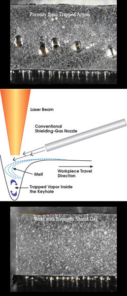
of a keyhole — a narrow, deep, vapor-filled cavity surrounded by molten metal
(Figure 3). As the laser moves across the work material, liquid metal flows around
the cavity, solidifying behind it. A flow of shielding gas is used to cover the
solidifying melt, to prevent oxidation and to reduce plasma problems at the keyhole
entrance, at least in theory.

Figure 3. In deep-penetration welding with conventional shielding-gas application, vapor
trapped in the keyhole can cause porosity. Successful processing with diode-pumped
solid-state lasers requires careful choreography of machining parameters, laser
specifications and shielding-gas application. Courtesy of IVF.
Resolving porosity
Researchers at IVF Industrial R&D Corp. in
Mölndal, Sweden, say that if the temperature of the plasma cloud is higher
than that of the vapor inside the keyhole, the net pressure is directed toward the
bottom of the keyhole.2 When the keyhole closes, trapped material can cause porosity.
Resolving this issue involves the careful choreography of several factors, including
processing speed, focal length of the optics and shielding-gas delivery.
The scientists recently explored the
use of both nitrogen and argon shielding gas in an application that involved laser
welding 6-mm-thick low-carbon stainless steel. Processing parameters for the test
bed’s Rofin-Sinar diode-pumped Nd:YAG laser included 3 kW of output power,
focusing optics with a 160-mm focal length and a 0.32-mm focal-point diameter. Both
gas types were tested at diverse welding speeds (5 to 16 mm/s) and gas flow rates
(10 to 50 l/min), using either a conventional nozzle trailing the laser beam or
a modified version that covered both keyhole and welding zone.
Results included solid welds at 10
mm/s with the modified nozzle and nitrogen shield gas. Where argon produced porosity
in the weld, nitrogen reportedly offered better shielding because of its higher
ionization potential and thermal conductivity. Moreover, the researchers surmise
that, because of nitrogen’s relatively high solubility in chromium steels,
porosity would be limited, even with gas trapped in the keyhole.
Exploring economics
Ultimately, said Richard Walker, president of
Cutting Edge Optronics in St. Charles, Mo., end users are increasingly considering
more than just up-front kilowatts per dollar when specifying diode-pumped technology.
Instead, they often give equal weight to long-term operating expenses.
David Peck at Trico Products Corp.
of Rochester Hills, Mich., recently faced such issues. The manager of advanced
products and processes R&D, he spearheaded a project to design and build a flexible
laser manufacturing system for high-volume processing of automotive wiper blades.
Design plans called for a cold rolled mill to produce each part with tapered thickness
from a fully annealed coil of spring steel, followed by continuous-contour laser
profiling of the part width, in-line hardening and tempering.
The goal of the line was a continuous
processing flow, with parts attached in a long ribbon-like manner from the point
where the raw material is pulled from the coil to the cleaning and painting stage.
The system was designed to operate at 10 m/min, with a coil lasting more than 50
hours. There would be no hard tools, and software control would be critical to assigning
every part a number without stopping or slowing the machine. The laser-based system
would replace a process involving progressive dies, injection molding, cold heading
and manual assembly.
The final design came down to either
a 2.2-kW diode-pumped Nd:YAG laser with fiber optic beam delivery and a 50/50 laser
beamsplitter, or two CO2 systems that required three times the footprint width.
The plan was influenced by a decision to reduce the required laser spot size from
400 to 300 μm, thus lowering power requirements, but the overriding issue remained
the firm’s wish for three additional processing lines down the road. With
the CO2 option, Peck said, the engineers would have needed to find a new location
for equipment after installing just the second line.
“Back in 1999, when we began
our project,” he said, “watt for watt, the diode-pumped laser system
was more expensive. Nevertheless, since we would have needed two CO2 lasers, the
up-front cost of the solid-state laser system was only 13.6 percent higher. When
comparing operating costs, we projected a savings of $12.74 per hour with the solid-state
laser system at full power. Ultimate payback was calculated at less than two years.”
For many applications, the benefits
of diode-pumped lasers will not be as obvious as they were for Peck. Engineers at
Quantronix Corp. of East Setauket, N.J., for instance, report that, at 100 W and
a 10-kHz repetition rate, a multimode second-harmonic Nd:YAG laser can cut through
a 1-mm-thick printed circuit board at about 250 mm/min. Cuts are of sufficient quality
whether the laser is lamp- or diode-pumped.
Now consider laser welding of plastics.
Kevin Hartke, product manager at Spectra-Physics in Mountain View, Calif., said
that there are several ways to apply laser light to the joint, including direct-write,
galvanometer, fiber array and mask techniques. With most, direct-diode and diode-pumped
lasers will work equally well. Where Hartke gives diode-pumped technology an edge
is in galvanometer-based processing. Again, beam quality is the deciding factor.
Final factors
As diode-pumped lasers continue their advance
into a variety of markets from scientific to materials processing, Jim Hopkins,
vice president at Coherent Inc. in Santa Clara, Calif., sees beam quality and the
ability to solve critical machining problems giving the technology an edge over
its competition. “Beam quality is a major issue. … Cost is always a
complaint, but at the end of the day, optical quality remains more important.”
Often, simple market economics will
dictate the laser solution. Bob Schricker at Lee Laser in Orlando, Fla., believes
that many of the diode-pumped solid-state lasers supplied by his firm to marking
OEMs will make their way to Southeast Asia, partly because that is where the bulk
of electronics marking applications are. The equipment’s reduced demands for
water, electricity and floor space only help the situation.
In the long term, issues such as system
footprint will become more critical as laser technologies continue their inroads
into new applications, whether in the micro- or macromachining world. According
to one estimate, a CO2 for deep-penetration welding to the degree of, say, 30 mm
might need to be room size. The required diode-pumped solid-state system would probably
fit on a large desk.
References
1. M. Grupp, T. Seefeld and G. Sepold (2001).
Laser welding of aluminum alloys with diode-pumped Nd:YAG lasers. ICALEO Proceedings,
LIA.
2. C. Lampa, M. Nilsson and B. von
Brömssen (2001). High-power diode-pumped Nd:YAG laser welding of medium-section
low-carbon martensitic stainless. ICALEO Proceedings, LIA.