Lessons learned from the telecom industry have helped fuel efforts to produce smoother, lower-cost coatings for a variety of commercial applications.
Hank Hogan, Contributing Editor
Over the past few years, the need to pack more telecommunications channels into a given swath of optical spectrum has forced manufacturers to offer deposition equipment that produces less costly and more uniform optical coatings. Although the pace of technical innovation has slowed, it has not stopped. New developments promise even smoother and less expensive optical coatings, many of which are useful for a number of consumer applications in addition to telecommunications. A look at them reveals where deposition technology is headed and where possible solutions to various problems lie.
Fred Van Milligen is vice president and chief technical officer of the Santa Rosa, Calif.-based thin-film products group of JDS Uniphase Corp. He has ridden the industry roller coaster, from the highs when equipment struggled to keep up with the telecommunications boom to the lows when vendors scrambled to find new uses for suddenly idle coating gear. Today, efforts are focused on cutting costs through improved productivity and better yields.
“One of the really driving requirements right now is defects,” he said. “It’s always important to improve cycle time. It’s always important for us to improve yields.”
He added that more and more applications, such as the windows, filters and mirrors found in cell phones and high-definition televisions, demand low-defect optical coatings at consumer-friendly prices. But producing such coatings in large quantities and over large substrates isn’t a trivial process. Recent advances in deposition technology promise to make the task a bit easier. Some of these innovations come from industry, some from universities and some from the efforts of large research consortia. All are potentially significant improvements; all have drawbacks.
New sources
On the industry side, a number of companies develop thin-film coating techniques and make optical components based on those coatings. JDS Uniphase is one, as is Bookham Technology plc of Abingdon, UK. Companies such as these make innovations in the optical coating deposition arena, but frequently they try to keep these improvements to themselves so as to gain a competitive advantage.
For example, earlier this year, Bookham acquired Cierra Photonics of Santa Rosa, Calif., which has since become the company’s thin-film products group. The group helps produce high-stability optical filters, devices that pass signals by relying on narrow-width filters that sit at precise frequencies. The narrower the width, the more closely the signals can be packed and the more channels system can handle.
Because a narrow filter is difficult to manufacture Bookham uses what it calls an advanced energetic deposition process. The company claims that this proprietary approach, which is in its third generation in as many years, improves yield because of greater film uniformity over an entire wafer substrate. However, those enhancements aren’t for public discussion, according to Dennis Derickson, product marketing manager for the thin-films group.
One company that does disclose details is Leybold Optics GmbH of Alzenau, Germany. At the Advances in Optical Thin Films conference in Saint-Etienne, France, last summer, Leybold unveiled a commercial product that reportedly promises to double the optical coating deposition rate without sacrificing film quality. According to company officials, this is partially due to a new plasma-ion-assisted deposition source. Dubbed the APSpro, it will be commercially available in Leybold coating equipment starting with the new year. The cycle time through the machines will be less than in the old ones, where cycles could take 10 or more hours, depending on the application. With the new source, that time will decrease by about a third.

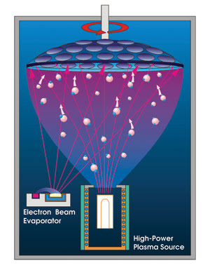
In a plasma-ion-assisted deposition process, an electron beam evaporates material to be deposited while a high-power plasma source provides additional energy. A substrate bearing plate rotates above the evaporator and source. Courtesy of Leybold Optics.
The key to the speedup is careful monitoring of the deposition and the newly developed plasma source. Consisting of a cylindrical cathode surrounded by a tube-shaped anode, this source works in conjunction with an electron beam evaporator, with the plasma assisting the deposition process. During operation, a voltage is applied between the cathode and the anode, igniting a discharge. Because of the design and the materials used, the result is an electrically balanced, effective ionization of the gas passing through the source.
The source also can run at higher power than previous versions. As a result, the energy of the plasma is greater and more effectively coupled to the gas, the deposition process and the film deposited on the substrate. Improved processing efficiency affects the deposition rate and film characteristics. However, because these films are typically oxides, it also is important to add oxygen to the deposition gas mix.
“If you expose these films to a plasma or ion beam consisting of argon ions, that leads to an improvement of the film properties because argon is a heavy ion. It bombards the film, then smoothes and densifies the film. But it also removes some oxygen, and so you need to add oxygen to get a fully oxidized film,” said Michael Sander, business unit manager for Leybold’s precision and telecom business.
Another important point, Sander said, is that the plasma allows a uniformly distributed transfer of energy to the deposited layers. That leads to an even coating process without the need to heat the substrate, making it possible to coat plastic and other low-temperature materials. Leybold Optics, which originally began developing the source during the telecom boom, plans to exploit such advantages and to expand into the precision optics arena for uses such as dichroic filters.
One atom at a time
Another coating technology innovation comes out of academic research and yields a similar twofold improvement — although, in this case, the increase concerns atomic layer deposition. This commercially available technique involves a two-step process. In the first phase, a vapor reacts with a surface until an atomic monolayer has been chemisorbed. The reaction is self-limiting and stops when the entire surface is covered. Then a second vapor reacts with the resulting surface in another self-limiting reaction. Again, the process stops when everything is blanketed. Because it leaves the surface in a state identical to its original condition, the second reaction completes the cycle and prepares the way for the process to repeat as needed.
Today atomic layer deposition processes are used to make electroluminescent flat panel displays, computer memory chips and components for disk drives. They also are being studied for other applications in semiconductor manufacturing.
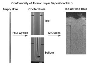
They offer a number of potential advantages over other coating methods. The film thickness can be dialed in with monolayer and, hence, 0.1-nm precision. Uniformly thick coatings can be deposited over large areas and rough terrain. The self-limiting nature of the reactions ensures that the process continues down deep holes, up steep sides and around curved surfaces. Likewise, the self-limiting aspect makes the process largely immune to differences in reactant flows and concentrations.
But what atomic layer deposition doesn’t offer is speed. A typical monolayer deposition cycle takes only a few seconds, but that means that the deposition rate hovers around 2 nm per minute. For a silica film, getting to the 100 nm or so required for a quarter wavelength of the visible spectrum means that the deposition time runs about an hour. Optical applications may require as few as two to as many as several hundred alternating high- and low-refractive-index λ/4 layers. This need has rendered the process impractical for many optical uses.
That may soon change with news of an improvement that effectively doubles the deposition rate. Research by Roy Gordon and colleagues in the chemistry department at Harvard University in Cambridge, Mass., reveals that part of the process, the low-refractive-index segment, can have its deposition speed boosted by orders of magnitude. The group has already demonstrated deposition of a 12-nm layer in a 15-second cycle, or roughly 30 times faster than the previous rate. Ongoing research indicates that even higher deposition rates are possible.

Atomic layer deposition enables uniform coatings, even down deep holes, as seen in this micrograph. Recent advances promise to cut process deposition times for optical layers in half, making the process more useful for optical applications. Courtesy of Roy Gordon, Harvard University.
“By some further optimization of the temperature, we can now — I think pretty reproducibly — go up to about 15 nm for a cycle,” Gordon said. He added that a commercial machine could probably cut the cycle time in half, from 15 to seven or eight seconds. Thus, the technique, which is being investigated by a number of companies, could allow a λ/4 film to be deposited in less than a minute.
The key is Gordon’s discovery of a silicon-based polymerization process. As in traditional atomic layer deposition, this method starts with a surface peppered with an appropriate seed, such as aluminum. The silicon in the reactant gas attaches to the seed and grows out in a silicone polymer fashion. That leads to deposition of not one unit, but as many as 30 or 40 at a time. The process stops when the different polymer chains cross-link. When done at the correct temperature, about 225 °C, the process is fast and leads to uniform coatings.
Unfortunately, because it requires a heavy infusion of silicon, the resulting oxides have low refractive indices. Thus, the process is not a complete solution to atomic layer deposition’s problems in making optical coatings. “We don’t have any equally high-rate process for the high-refractive-index material. Those are still quite a bit slower. So that’s right now the bottleneck, or the slow step in making an alternating set of films,” Gordon explained.
Mirror, mirror
The extreme ultraviolet (EUV) presents another area where coating speed and film properties are being pushed to the limit. State-of-the-art semiconductor feature sizes are less than 100 nm and getting smaller. The industry consensus is that advances must be accompanied by a shift to shorter-wavelength light sources. Today’s leading-edge manufacturing technology uses a 193-nm light source. The chosen wavelength for tomorrow’s technology is about 13.4 nm. The problem is a lack of material with reasonable transmissivity at such a wavelength.
“We are forced to rely only on reflective approaches — mirrors,” said Phil Seidel, a project manager in the lithography division at International Sematech in Austin, Texas. The research consortium, along with its industry member companies and supplier partners, is working on ways to produce the required optical components and lithography process.
With significant research and development still to be done, the preferred approach at the moment is to use λ/4-stack multilayer reflection. This involves as many as 40 alternating layers of materials — a molybdenum stripe roughly 4.1 nm thick and a silicon film approximately 2.8 nm thick, for example — chosen at least partially based on their different refractive indices. Incident light at the 13.4-nm wavelength is both transmitted and reflected at each stack interface. The reflection constructively interferes. With optimization, reflectivity of the target wavelength has been shown to be greater than 70 percent.
The issues involved in this thin-film coating include off-peak reflectivity, as well as layer smoothness, stability and defectiveness. On the latter, Seidel noted that the industry is at least an order of magnitude away from the mass-production requirement of less than 0.006 defects of 30-nm diameter and above, per square centimeter, on an EUV lithographic mask.
One of the companies working in this area is Veeco Instruments Inc. of Woodbury, N.Y., which makes a low-defect density ion beam deposition device for coating the 6-in. mask blanks used in the EUV. The device can produce mask blanks, but there are some stringent requirements to be met. According to Dan Abraham, vice president of advanced development for the process equipment division, a high degree of coating uniformity is needed for production. “We are looking at a subpercent uniformity number,” he said.

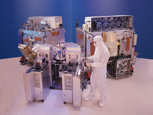
Operating at wavelengths of 13.5 nm, the next-generation semiconductor photomasks require complex yet uniform, defect-free optical coatings. Coatings such as this are produced by this low-defect-density ion beam deposition system. Courtesy of Veeco Instruments Inc.
Abraham reported that, in collaboration with Sematech and the Albany Nanotechnology Center of Excellence, Veeco recently demonstrated mask-blank reflectivity high enough to satisfy a standard established by the consortium. He added that the company is pursuing ways to reduce defects in the mask-blank process.
Germany’s Fraunhofer Institute has its own ideas about how to meet the coating requirements. Based on the campus of Michigan State University in East Lansing, Fraunhofer USA’s coatings technologies group is pushing a pulsed-laser deposition process. As do other approaches, this needs further development before wide-scale production can be undertaken.
It’s possible that some of that research and effort will lead to a two-way exchange. Coating advances are needed to create the mask blanks. But at the same time, coating technology is being increasingly driven by the need to cut costs, improve throughput and eliminate defects. That’s strikingly similar to the demands made on the semiconductor industry, and so the technology traffic may not all flow from the coating industry to the EUV lithography needed for tomorrow’s integrated circuits. Tutoring may go in the other direction as well.
As Van Milligen noted, “The low-defect lessons of the semiconductor industry are becoming more and more important to the optical coating industry.”