With integrated photonics, gone is the tedious, expensive and error-prone manual connecting of components, thanks to integration that brings these onto a single chip.
When it comes to spacecraft, planes and military gear, weight is all important. That’s understandable, as it costs about $10,000 to put a pound in orbit, in the case of spacecraft. For planes and military gear, there are limits on what can be flown or carried. Hence, the importance of keeping weight down — and the growing interest in and use of photonic integrated circuits (PICs).
“We’re buying size, weight and power,” said Michael Krainak of the technology.

Measuring strain with fiber optics allows computation of wing deflection and slope, which can be used for structural health monitoring, active drag reduction and active flexible motion control. NASA researchers have come up with a way to do this using only one wire per fiber optic strain sensor. Courtesy of NASA.
Krainak is head of the laser and electro-optics branch at NASA Goddard Space Flight Center in Greenbelt, Md. He is also NASA’s liaison to the American Institute for Manufacturing Integrated Photonics, a Rochester, N.Y., joint public-private initiative that has funding from the U.S. Department of Defense and elsewhere.
What integrated photonics enables is the mass production of devices. Gone is the tedious, expensive and error-prone manual connecting of components, thanks to integration that brings these onto a single chip. Another plus is that putting everything on a chip fabricated in a cleanroom eliminates dust, which scatters light and consequently degrades photonic signals.
Sensing machine health and more
In an October 2016 presentation, Krainak said that the areas where photonics could help aerospace include sensing and communications. Defense application areas are the same, although military uses will also likely include remote detection of chemical and biological agents as well as explosives, Krainak added in a later conversation.
In discussing sensing, Jose Pozo, director of technology and innovation at the European Photonics Industry Consortium, pointed to lidar, which measures distances by sending out laser pulses. It is useful in missile guidance and tracking, autonomous flight, and aircraft damage detection. Implementing this technology using photonic integrated circuits would cut size and cost.
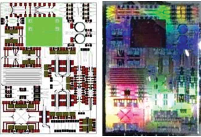
Photonics integrated circuit for deep space laser communications. Courtesy of Johathan Klamkin, UCSB.
“Using PICs for the optical beam steering of laser light without the use of moving parts has become a key development for such a purpose,” Pozo said.
Other promising applications include optical gyroscopes, with researchers at City University of New York coming up with a scheme in 2015 for one that only measures a fraction of a millimeter and thus could potentially be incorporated entirely onto a chip1. Other sensing applications could involve optical accelerometers and multiwavelength imagers.
Vehicle health monitoring applications are also important because airplanes, spacecraft and military vehicles are subject to repeated and sometimes violent movement, which causes strain. This can be measured by writing a Bragg grating into an optical fiber and then attaching the fiber to the component of interest.
“A fiber Bragg grating reflects one part of the light. If you stretch this grating, you will get a slight change of the reflected light. That is what we are looking at and basically you do that with a narrow band spectrometer,” said Pim Kat, president and CEO of the Technobis Group. Located in Alkmaar, the Netherlands, the company concentrates on aerospace and medical applications.
In the past, this measurement has been done using free space optics, which leads to large, heavy, expensive and power-hungry systems, as compared to what’s possible with photonic integrated circuits. Richard Visser is CEO of Smart Photonics BV, an Eindhoven, Netherlands-based foundry that works exclusively in indium phosphide. He said that the integrated strain-measuring chips are only a few square millimeters in size, making them much smaller and lighter than the free space optics equivalent.
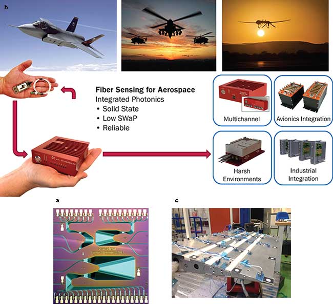
Optical chips (a) detect strain and/or temperature changes via fiber Bragg gratings, enabling health monitoring of wings (b) and other structures. They also can be used to help monitor and control structures that change shape, as shown in this demonstrator (c) of an adaptive trailing edge that morphs into different shapes to improve aerodynamic performace. Courtesy of Technobis.
“They are also thousands of times more accurate due to a lack of vibration effects,” Visser said.
Because of these characteristics, systems built using integrated components can be deployed in more places aboard a vehicle. This means its health can be more closely monitored, which is of interest to both civilian and military aircraft makers and users.
Communication benefits
As for communications, an important point about optical beam steering is that it offers an advantage beyond simply getting rid of mechanical parts that can fail, according to Paul van Dijk, vice president for strategy and innovation at LioniX International, a pure-play integrated photonics foundry based in Enschede, Netherlands (see also Marie Freebody’s “Medicine and the Life Sciences” on p. 54). The company recently absorbed van Dijk’s previous enterprise, satellite-to-airplane communications systems maker Satrax BV.
Photonic-based beam steering allows Satrax to connect planes in flight to satellites while replacing a domed enclosure that protrudes from the plane with one that is flush with its skin. This lessens drag on a plane and improves its aerodynamics. This would save airlines around €100,000 ($109,000) in fuel costs a year, based on van Dijk’s calculations.
Photonic integrated circuits enabled Satrax to take discrete components and modules that are shoebox-size and put them all on a chip as big as a coin. “We came from the sizable unit with lots of fibers and discrete modulators and detectors to a design with on-chip functionalities, reducing size, weight and making it robust and compact,” van Dijk said.
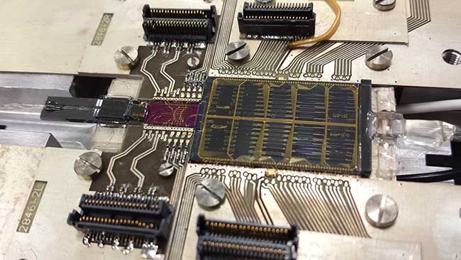
Integrated photonic beamformer with steering through time delays. On-chip modulators (the purple color) are built using InP with a beamforming network in silicon nitride-silicon dioxide (Si3N4-SiO2). Courtesy of Satrax.
This beam steering for external communication is done using microwave photonics. Communication within an aircraft or military vehicle could be over fiber optics, with signals that are insensitive to electromagnetic interference and cross talk.
Integration offers a 10- or 100-fold reduction in size, as well as a significant savings in weight, said Iñigo Artundo, CEO of independent design house and manufacturing services broker VLC Photonics of Valencia, Spain. He noted that there also can be a substantial performance boost with a cost and power consumption decrease, as compared to what’s possible with discrete components. However, those cost savings somewhat depend upon volume production, something that rarely happens in aerospace and defense applications.
This means that it may make more sense to piggyback on developments originally intended for other areas, like telecom or data centers. If this can be exploited, then aerospace and defense applications can benefit from the economies of scale created by such large markets.
Challenges in validation, materials and more
However, that could prove difficult because aerospace and defense have exacting requirements when it comes to packaging and testing. “The biggest challenges to overcome are surely on the validation and certification of photonic integrated circuits for these markets, as procedures and standards are very important here, operation under harsh environments is critical, and significant investments are required,” Artundo said.
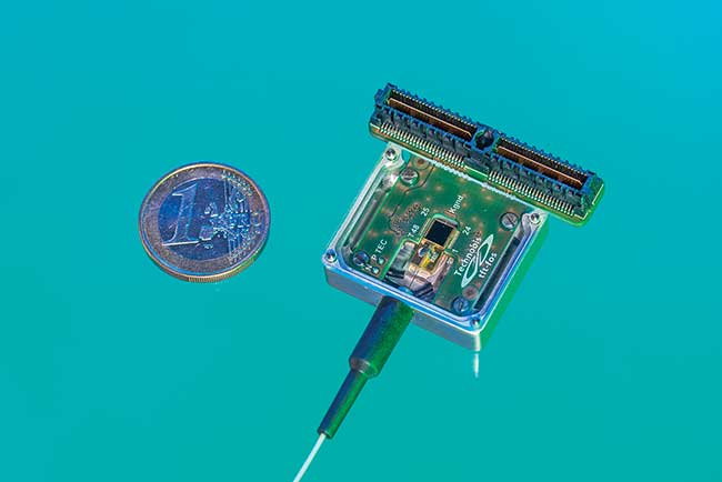
PIC is considered to be the most promising technology for the next generation of interrogation devices for fiber optic sensing. In the picture is a packaged PIC-based fiber sensor interrogator developed by Technobis. Courtesy of Technobis Group BV.
Another challenge for photonic integrated circuits in general is there is no single material system suitable for all applications, with silicon, silicon-on-insulator, silicon nitride and indium phosphide all popular substrates. Silicon, which is dominant in electronics, is used for passive components, detectors and modulators. In contrast, indium phosphide enables electrically pumped amplifiers and lasers. However, it is expensive and users cannot exploit silicon’s vast manufacturing base.
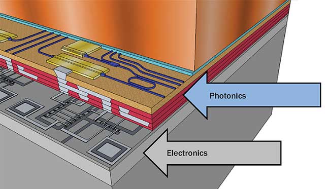
Future photonic integrated circuits may take a hybrid approach, using silicon as a substrate for electronics and another material for the photonics. Courtesy of Katarzyna Lawniczuk, Edinhoven University of Technology.
Solutions under evaluation include growing indium phosphide on a silicon substrate or putting a chip of it directly atop a silicon one. The future is likely to be a combination of both approaches, with CMOS silicon used for the electronics and other materials for photonics, said Katarzyna Lawniczuk, photonic integration group project coordinator at the Eindhoven University of Technology in the Netherlands.
“There will be more of the hybrid solution with electronics and optics than single optical photonic functionality,” she predicted.
On the other hand, NASA’s Krainak noted that optical gain materials can be built using CMOS-compatible processes. For instance, Laura Agazzi and colleagues in a 2010 Optics Express paper2 reported using erbium-doped aluminum oxide as a gain medium that can be optically pumped. They fabricated demonstration devices in a CMOS pilot line. There is the possibility that a CMOS-compatible gain material could be electrically pumped. More materials and device architecture work is needed to further explore the limits and possibilities of this approach, Krainak said. Having a single material platform could help cut costs, as has happened in electronics.
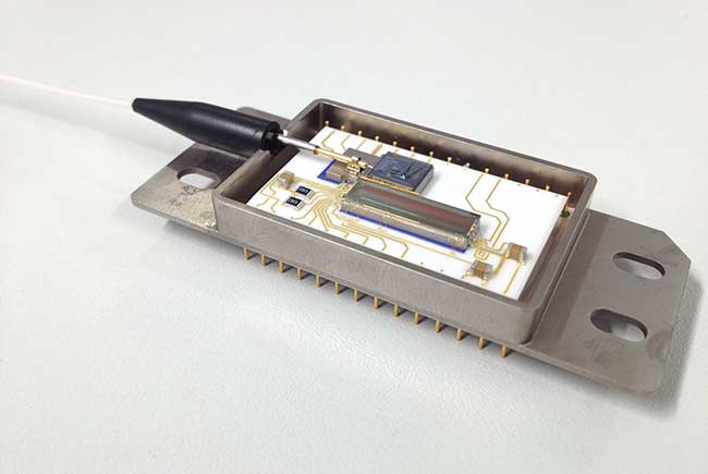
Because they are lightweight, robust and offer better performance, integrated photonic devices like the one pictured above are used in space and harsh environment sensing applications. Courtesy of Tyndall Institute.
A final issue that confronts photonic integrated circuits is packaging. Peter O’Brien, head of the photonics packaging group at the Tyndall National Institute of Cork, Ireland, said that future manufacturing needs to be done passively, as opposed to active packaging. The latter looks at the output of the device and then tunes the alignment and other packaging parameters to get the best signal. It’s a method that costs more and has a lower throughput than a passive approach, but it is currently necessary.
The situation may change, thanks to research and development at Tyndall and elsewhere. That may lead to a different manufacturing flow than is used today. “That will be wafer scale, with passive processes as opposed to active, using an electronic assembly manufacturing process that is machine vision based, for example,” O’Brien said.
He added, though, that a premium is placed on performance and reliability in aerospace and defense applications. Therefore, manufacturers of these products may opt
to go with a more expensive approach because of what it buys, particularly in terms of improved reliability.
References
1. L. Ge and R. Sarma, et al. (2015). Rotation-induced evolution of far-field emission patterns of deformed microdisk cavities. Optica, Vol. 2, Issue 4, pp. 323-328.
2. L. Agazzi and J.D.B. Bradley, et al. (2010). Monolithic integration of erbium-doped amplifiers with silicon-on-insulator waveguides. Optics Express, Vol. 18, Issue 26, pp. 27703-27711.