Integration and packaging of optical components such as laser sources, multiplexers, detectors and modulators into a single chip are ushering in a new era of communications to 100 Gbps and beyond.
Today’s data centers deliver millions of services, processing terabytes of data per second around the world for billions of devices. Considering the volume, it’s amazing that we ever have a signal. As the need for connectivity increases, data centers are under constant pressure to add more and more massive racks of servers and fiber optic interconnects, which takes money and time, energy and real estate.
The demand for large-scale cloud computing and ever-faster processing is growing so fast that network traffic in data centers is doubling every twelve months, according to Diane Bryant, vice president and general manager of data centers at Intel.1 And copper wires struggle to transmit at data rates of 25 Gbps over a few meters, says Microsoft’s general manager of hardware engineering, Kushagra Vaid. “As data rates start getting to 100 Gbps — and this will happen in the future — we are going to hit a brick wall,” Vaid said.

Many experts in government, industry and academia predict that photonics integrated circuits (PICs) — chips that integrate photonics components alongside the electronics — will be an important part of the solution. These monolithic PICs will improve upon today’s vertical-cavity surface-emitting laser (VCSEL) technology, in which VCSELs are coupled to the chip via multimode optical fiber links, but are bandwidth-distance limited. After decades of research and development, the public is finally getting a glimpse of what viable PIC solutions might look like (Figure 1).
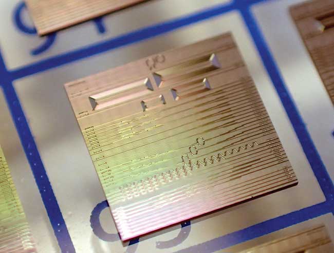
Figure 1. A prototype SiN photonics integrated circuit fabricated at Ligentec (Lausanne, Switzerland)is one example of a better, smaller, faster chip that will introduce economies of scale in future telecom and datacom build-outs. Courtesy of VLC Photonics.
In August, Intel officially introduced a commercially available silicon (Si) photonics transceiver for data center network switches at the Intel Developer’s Forum in San Francisco (Figure 2). In development for 16 years, Intel claims its QSFP28 switch-to-switch interconnect is the first product to integrate a hybrid indium phosphide (InP) laser directly into the silicon. The PIC-based platform can handle data rates of 100 Gbps over 2 km of singlemode fiber, leveraging wavelength division multiplexing and lower power requirements to allow data centers to scale to 400G modules in the future. Microsoft is already a customer; other targets include Facebook, Google, Amazon and Alibaba.
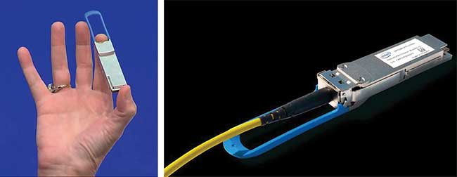
Figure 2. Sixteen years in the making: Intel’s Bryant announces the first commercially available Si photonics platform at the Intel Developer Forum in San Francisco in August. Right: Intel claims the 100G PSM4 (parallel single mode fiber 4-lane) QSFP28 optical transceiver is the world’s first commercial Si photonics chip to feature a fully integrated InP hybrid laser. Courtesy of Intel.
Scaling via packaging
Multinational giant IBM, based in Armonk, N.Y., isn’t far behind with another PIC-based solution for data centers and cellphone towers, using a different approach. In 2015, researchers at IBM announced the successful testing of a fully integrated wavelength division multiplexing (WDM) Si photonics chip for Big Data and cloud services, enabling the download of an entire HD digital movie in two seconds (Figure 3).
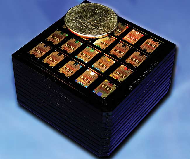
Figure 3. Several hundred monolithic chips incorporating optical and electrical circuits are combined in a cassette to demonstrate 100-Gbps transmission suitable for deployment in cloud servers, datacenters and supercomputers. Courtesy of IBM.
According to Tymon Barwicz, Ph.D., researcher in Silicon Nanophotonic Packaging at IBM Thomas J. Watson Research Center in Yorktown Heights, N.Y., the PIC program at IBM has two parts: the first is the finessing of the wafer fabrication using existing CMOS fabrication processes (a business licensed to GlobalFoundries in 2015 when the company acquired IBM’s semiconductor business), and the second is the packaging of the photonics using existing high-throughput microelectronics assembly facilities.
“The IBM wafer technology integrates the photonic devices and transistors side by side on the same chip,” said Barwicz. “We can now make a photonics integrated chip in a standard CMOS foundry, notably reducing its cost.”
In addition, IBM is leveraging the existing pick-and-place tools from high-volume microelectronics packaging to do the photonics assembly instead of using expensive custom automated tooling or manual assembly lines.
“Our approach was to say, hey, the same way we applied microelectronics fabrication for PICs can be used in photonics circuit packaging, with a big cost and yield advantage,” said Barwicz.
The challenge was to overcome the inaccuracy of high-throughput pick-and-place machinery (with +/− 10-µm accuracy) to align fibers with 1- to 2-µm accuracy2. Mode engineering and self-alignment schemes were able to overcome the placement problem. Then the machines were fit with customized vacuum pick tips and chip holders to enable photonic assembly. The result will be a scalable, cost-effective photonic packaging technology that doesn’t rely heavily on manual labor. Today, the project is close to commercialization; no timetable has been announced, but the technology is in the reliability and yield stage.
PIC partners
Big multinational innovators like Intel, IBM and Cisco are working hand in hand with partners in business, academia and government to develop PIC-based solutions to communications challenges. For smaller enterprises, public-private partnerships have forged national research consortiums like the American Institute for Manufacturing Integrated Photonics (AIM Photonics, Rochester, N.Y.) in the U.S., and the European Photonics Industry Consortium (EPIC, Paris) in Europe. These innovative initiatives have sprung up to provide a manufacturing infrastructure, support, partnerships and financial assistance — with PIC development in mind.
With members encompassing the entire value chain of photonics, EPIC works with companies like VLC Photonics, a fabless PIC design house in Valencia, Spain, to help customers in industry and academia with early PIC concepts, and then assist them in development all the way to pilot production and beyond.
The nonprofit AIM Photonics, sponsored by the U.S. Department of Defense and managed by the State University of New York (SUNY), announced in October a new Tier 1 industry member, Infinera, a pioneer in InP lasers on PICs. Infinera is offering its resources and expertise in large-scale PICs and packet optical convergence to other members — all for the purpose of leveraging past success in electronics into the acceleration of integrated photonics for lower power, smaller-area networks.

Figure 4. Michael Krainak, head of integrated photonics at NASA’s Space Technology Research Grants Program, and head of the Laser and Electro-Optics Branch at NASA/Goddard Space Flight Center, holds the PIC that will be demonstrated as a key communications capability for future spacecraft. Courtesy of NASA.
PICs in space
Another AIM Photonics partner, NASA, is heavily involved in Si photonics R&D for its communications needs (see also “In Defense and Aerospace” on page 62). Earlier this year, the U.S. space agency announced plans to build the first integrated photonics modem for use on the International Space Station as part of NASA’s multiyear Laser Communications Relay Demonstration (LCRD)3. The modem, named the Integrated LCRD Low-Earth Orbit User Modem and Amplifier (ILLUMA), will incorporate lasers, encoders, optical switches and transmitters on a single chip, designed for eventual high-speed laser communications from Earth to spacecraft all over the solar system (Figure 4). The technology, scheduled for testing in 2020, will be made available to industry and other government agencies in the future.
PICture this
One of the steepest challenges to widespread adoption of PICs is incorporating lasers into the chip. More than one material may emerge as a winner for use in hybrid lasers on PICs. Silicon itself doesn’t lase, although adding a layer of a III-V material helps overcome that limitation; Intel added InP, for example. But III-V materials are inherently not compatible with conventional CMOS fabrication, leading to expensive work-arounds. Research is hot on the trail of graphene, a two-dimensional layered material that can emit, transmit and detect photons, but issues of CMOS scalability and performance are handicaps that will take time to overcome4.
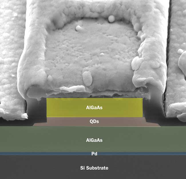
Figure 5a. SEM image of an InAs quantum dot (QD) laser on a Si substrate using low-temp Pd wafer bonding reveals an AlGaAs cladding and metal contact top layer. Courtesy of Z. Wang, RIT. Courtesy of Z. Wang, RIT.
One lasing material showing great promise is quantum dots (QDs) (Figure 5). Recently, researchers at Rochester Institute of Technology (RIT, Rochester, N.Y.) demonstrated that indium arsenide (InAs) QD laser heterostructures can successfully be grown and transferred to Si substrates via a low-temperature palladium (Pd)-mediated wafer bonding process (Figure 5a, 5b). Associate professor of microsystems engineering Stefan Preble and colleagues at RIT, in collaboration with professor Wei Guo at the University of Massachusetts, Lowell, further demonstrated mode-locking of these lasers, which would enable stable optical pulse trains of short pulses (<10 pc) at high repetition rates for optical time-division multiplexing (OTDM), among other uses (Figure 5c)5. The group is looking at schemes to combine wavelength division multiplexing (WDM) with OTDM to get to data rates beyond 400 Gbps. The biggest hurdle with QDs is efficiency, but their temperature stability is making them hot prospects for next-generation PICs.
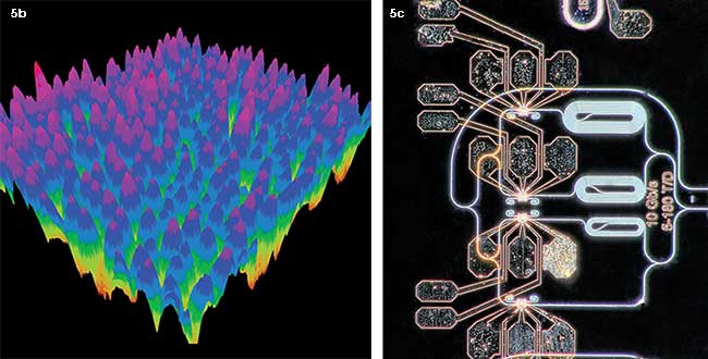
Figure 5b. This false color 3D atomic force microscope image shows the height profile of the InAs QDs on Si (at left). Figure 5c. The Si PIC generates optical time-division multiplexing signals at 40 Gbps from 10 Gbps QD mode-locked lasers (above). The circuit splits the short pulses from the laser into four separate paths, each modulated by Si ring resonator electro-optic modulators, delayed and recombined at the higher data rate of 40 Gbps. Courtesy of K. Tian and Z. Wang, RIT and M. Fanto, RIT.
“Quantum dots have recently been pulling ahead of quantum wells as a promising next-gen PIC solution,” said Preble. “The QD is less susceptible to defects that destroy performance over time. And several promising approaches for direct growth of QDs on Si chips are emerging. But the yield and long-term reliability of QDs on silicon remains to be proven.”
Other schemes beyond WDM and OTDM may someday be able to carry terabyte data rates on a single chip. Assistant professor of electrical engineering Liang Feng at the University at Buffalo, State University of New York, and colleagues recently demonstrated a tiny microring laser that emits photons in a radially polarized stream. The orbital angular momentum (OAM) of the photons creates a vortex shape that offers novel degrees of freedom and flexible control through on-demand topological charge and polarization states. The scheme may enable mode multiplexing over many orders (potentially an infinite number of orders) for tens of OAM channels6,7,8 (Figure 6). The OAM laser might offer entirely new ways of implementing high-speed, secure optical signals in both classical and quantum regimes.
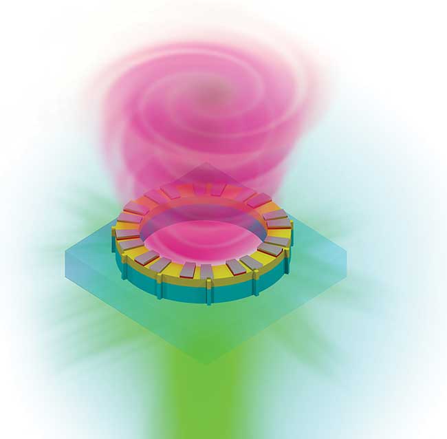
Figure 6. Structured helical wavefronts from a vortex laser could someday carry an unlimited number of orbital angular momentum modes for next-gen terabyte optical communications. Courtesy of L. Feng/Univ. at Buffalo.
“Fifty years ago you couldn’t have imagined what our everyday life would be like today,” said Feng. “The power in our laptops is as great as the supercomputers that helped put astronauts on the moon. We certainly have a very long way to go, but all over the world people are trying to increase the laser energy emission in photonic circuits. In the next 50 years, it’s exciting to imagine what we’ll accomplish.”
References
1. D. Bryant (August 2016). Data center: The center of possibility (video). Intel Developer Forum, San Francisco.
2. T. Barwicz et al. (November/December 2016). A novel approach to photonic packaging leveraging existing high-throughput microelectronic facilities. IEEE J of Selected Topics in Quan Elect, Vol. 22, No. 6.
3. S. Alt and J. Pellish (April 2016). Photonic integrated circuit (PIC) device structures, NASA Electronic Parts and Packaging
Program, NASA/Goddard Space Flight Center.
4. M. Wheeler (August 2016). For integrated photonics, a tale of two materials. Photonics Spectra, pp. 38-45.
5. Z. Wang et al. (October 2016). InAs quantum dot mode-locked lasers on a Si substrate by Pd-GaAs wafer bonding. Proc Frontiers in Optics 2016, Rochester, N.Y., paper FF5F.5.
6. P. Miao et al. (July 2016). Orbital angular momentum microlaser. Science, Vol. 353, Issue 6298, p. 464.
7. J. Wang et al. (May 2012). Terabit free-space data transmission employing orbital angular momentum multiplexing. Nat Photon, Vol. 6, p. 488.
8. N. Bozinovic et al. (June 2013). Terabit-scale orbital angular momentum mode division multiplexing in fibers. Science, Vol. 340, Issue 6140, p. 1545.