Increased throughput and tighter specs in consumer electronics spur innovations in line-scan cameras and the use of LEDs.
HANK HOGAN, CONTRIBUTING EDITOR
Every year, smartphones, TVs, tablets, and computers get more capable in terms of screen resolution and processing power. Better consumer electronics and more demand have led to volume increases. According to an October 2019 report from Kenneth Research, smartphone shipments will hit 2.97 billion in 2020.
At the other end of the scale of consumer electronics screen size, IHS Markit forecast that 226 million TVs would ship in 2019.
This deluge pressures manufacturers to increase throughput. So they must reduce how long it takes on average to
make one unit, an interval known as takt time.

“In a lot of consumer electronics, they need to improve takt time by improving how fast they can inspect what they’re inspecting,” said Mark Butler, head of product management at Waterloo, Ontario, Canada-based Teledyne DALSA. The company provides high-performance digital imaging solutions.
“And they also have to find a lot more defects than they did in the past,” he said.
This need to find more defects is a consequence of the rising performance of consumer electronics. Pixel counts are going up, but screen sizes are either staying the same or not increasing as fast. Consequently, pixel sizes are going down. Inspection designed to detect problems in these pixels must find smaller defects.

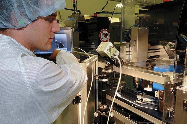
The speed of operations in consumer electronics may require high-speed vision systems for analysis of manufacturing. Courtesy of Mikrotron.
Something similar is taking place in printed circuit boards because, over time, more and more components must be squeezed together in the same space. As a result, killer defects — such as when a conductive trace line bulges outward to touch another line and cause a short — are evermore
difficult to spot.
Machine vision vendors are responding with various solutions to the dual trends of higher throughput and tighter specifications. Teledyne DALSA, for instance, makes line-scan cameras that are used to verify that printed circuit boards have all their components in place and that important features such as trace widths and spacings meet specifications.

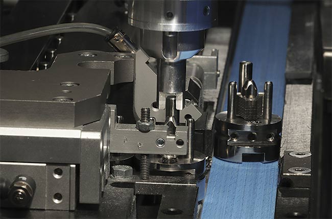
Vision systems are used to guide component pick-and-place processes and inspect the results. Courtesy of Mikrotron.
The company’s line-scan cameras are also used to check on the circuitry of flat panel displays. While the manufacturing process, device structures, and materials differ between LCDs and OLEDs, the two main consumer electronic display technologies use comparable approaches for some quality control tasks.
“You still need inspection machines for OLEDs or LCDs, and the requirements on the camera [in the inspection process] are very similar because high pixel densities and the desire to inspect faster remain,” Butler said.

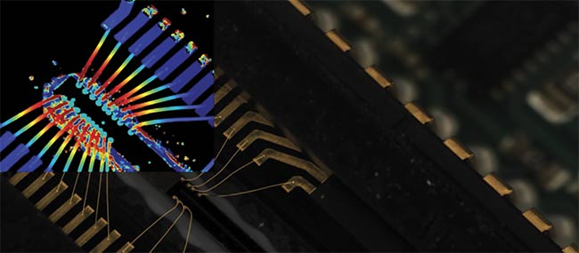
Depth sensing can improve quality control checks of the wire bonds that connect chips to consumer electronic circuit boards. Courtesy of Chromasens.
Teledyne DALSA’s newest multichannel line-scan cameras were designed to address the unique needs of consumer electronics manufacturing. This innovation consists of three separate, closely spaced line-scan channels in a single unit. Thus, the image captured by the first sensor may be separated from that of the second by a few lines, and the third would follow the second by the same spacing. Algorithms in the device can compensate for this spacing, if necessary. In this way, the resulting images can be co-registered with each other.
'Disruptive technologies such as digital twin, AI, neural networks, or
deep learning will be catalysts in the dramatic improvement of machine
vision’s automation capabilities,' — Alexander Bourgeois, IHS Markit Technology
Getting a throughput increase out
of this arrangement happens when
the camera is teamed up with various
colored LEDs and the appropriate filters are used in the multiline line-scan camera. For example, placing the camera above a printed circuit board illuminated by an overhead green LED enables a green-filtered channel to inspect the board. At the same time, shining a blue LED from below allows a blue-filtered channel to ensure that through holes are where they should be. Finally, a red LED angled to the side can highlight various defects to a red-filtered sensor.
With such an approach, a single camera can do the work of three, Butler said. Importantly from a throughput point of view, this capability means one inspection pass can potentially take the place of several others. So less time needs to be spent in a quality control check.
According to Butler, the inspection tasks often performed in consumer electronics manufacturing do not lend themselves to image processing on the camera itself. “It’s a very complicated image, so it’s very high frequency, lots of black, white, black, white,” he said.

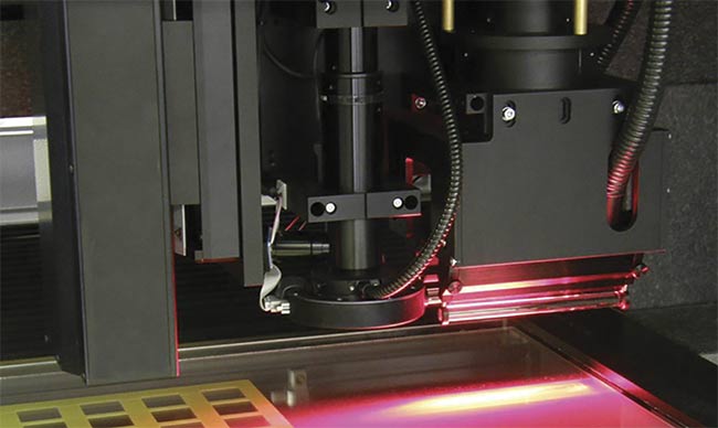
White light interferometry and high-speed cameras provide 3D data, enabling defect detection in consumer electronic components. Courtesy of Mikrotron.
Inspecting the thin-film transistors on an LCD display panel, for instance, takes place over a 5- × 5-pixel grid. In that space, the imaging requirements are to find three sets of transistors needed to produce a colored dot, and to determine the height of those devices. Since this must be accomplished at speeds that can exceed 4 gigapixels/s, the amount of processing is so great that it’s more economical to ship the data off the camera and process it elsewhere, Butler said.
While it may at times be best to process some image data remotely, at other times the shortest possible response time is important. Case in point: Some machine vision tasks in consumer electronics manufacturing are much the same in automobile or pharmaceutical production, said Stephen Ferrell, director of business development in the Americas for Mikrotron GmbH. The Munich-based company makes high-speed cameras and associated systems.
Ferrell said that in such high-speed, high-volume manufacturing, machine vision may monitor component or product transfer points, machinery operation, or the stacking, inserting, cutting, and trimming of product. These steps can take place rapidly, in times as short as milliseconds, requiring hundreds to thousands of frames per second to capture and analyze motion components.
FPGAs required
In such cases, processing in the camera or the local PC has traditionally been handled by a GPU or CPU. Mikrotron is pushing the use of field-programmable gate arrays (FPGAs) because the arrays offer a highly
parallel design that is well suited to
the steps needed in analyzing machine vision data.
“Image preprocessing, image segmentation, feature extraction, and image interpretation in both the spatial and frequency domains using linear and nonlinear filters can be performed in real time at hundreds or thousands of frames per second,” Ferrell said.

A close-up of a computer circuit board.
He added that this exceeds the rate performed with a CPU and that using FPGAs simplifies system architecture. In addition, if the FPGAs are located in the camera, they can be used for neural networks, enabling deep learning for extracting even more information from a given image.
Faster processing and better algorithms can indeed help meet the demand in consumer electronics manufacturing for higher throughput and improved quality inspections, according to Sam Lopez, vice president of sales and marketing for Montreal-based Matrox Imaging. A division of Matrox Electronics Systems Ltd., Matrox Imaging supplies grabbers, smart cameras, vision controllers, and image processing and analysis software.
According to Lopez, Matrox Imaging products are found in vision systems at all stages of the consumer electronics manufacturing process. He said the increasing complexity, such as higher pixel counts, of the products produced means vision solutions must evolve to keep pace.
“As the number of pixels is increasing and pixel sizes are decreasing, vision systems need to have the ability to scale to match these more precise requirements,” Lopez said. “This is achieved through systems that can accommodate higher and higher image resolutions.”
In addition to algorithms that improve the performance of vision systems, vendors may also have to implement hardware improvements. They may, for instance, use the latest processors in smart cameras and industrial PCs. In other cases, they may deploy new industrial standards, such as CoaXPress 2.0, that offer higher data transfer rates.
“Version 2.0 of CoaXPress has added two more speeds, 10 Gb/s (CXP-10) and 12.5 Gb/s (CXP-12), ideal for supporting higher-resolution cameras at double the speed of the original, without the complexity and cost of multiple cables and connectors, and in a platform that is easily adapted and scaled to meet rapidly changing requirements,” said Donal Waide, director of sales at Woburn, Mass.-based frame-grabber maker BitFlow Inc.
All these innovations may bring multiple benefits. According to Teledyne DALSA’s Butler, quality and cost affect each other. Getting rid of bad parts as soon as possible in the manufacturing process means less investment in product that eventually may be scrapped. So, better and more frequent inspections can bring several advantages.
“You can also improve your quality, and that will generally save you in cost,” Butler said.
Finally, in looking at the future of machine vision in consumer electronics
manufacturing, Alexander Bourgeois — a research analyst with IHS Markit Technology, which is now part of business-to-business information provider Informa Tech — said it was important to consider the impact of emerging technologies. These could someday make it easier to satisfy the dual needs of manufacturers for greater throughput and higher quality.
“Disruptive technologies such as digital twin, AI, neural networks, or deep learning will be catalysts in the dramatic improvement of machine vision’s automation capabilities,” Bourgeois said. These capabilities, combined with continued advancements in cloud computing, will help to handle the increasingly large amounts of data required in image processing, he said.
