The benefits of chalcogenides — their optical properties, low cost, and manufacturing options — continue to enable growth in the thermal/IR imaging market.
JEREMY HUDDLESTON, ANDREW LOCKE, AND ALAN SYMMONS, LIGHTPATH TECHNOLOGIES
As the thermal imaging market continues to rapidly expand, a broad array of commercial applications has placed an increased emphasis on balancing cost and performance. While some still perceive conventional materials and manufacturing methods of optical components and assemblies as tried and true, advancements in certain novel technologies, such as chalcogenides and precision glass molding, have dramatically changed the longwave-infrared (LWIR) landscape.
The evolution in thermal imaging was first initiated by the rapid commercialization of uncooled microbolometers for LWIR applications, beginning in the 1990s and early 2000s. At the time, this new, low-cost detector technology enabled order-of-magnitude price reductions, which meant optical lens assemblies were responsible for a disproportionate share of the overall cost of camera systems. With increasing price pressure, lens manufacturers were forced into a highly competitive environment of maximizing efficiency while chasing decreasing margins.

Image of a Porsche shot with a thermal lens assembly. Courtesy of LightPath Technologies.
For traditional lens manufacturers, this became an exercise in diminishing returns because of the limits of incremental process improvements along with the fluctuating global market for standard crystalline materials. In addition, the emerging commercial applications for low-cost thermal imaging created substantial increases in demand for volumes far exceeding the capacity of traditional low-throughput manufacturing methods and the availability of common materials such as germanium (Ge), zinc sulfide (ZnS), and zinc selenide (ZnSe). The market was primed for a game-changing and disruptive technology, and two enabling technologies merged to meet this challenge.
Chalcogenide glass
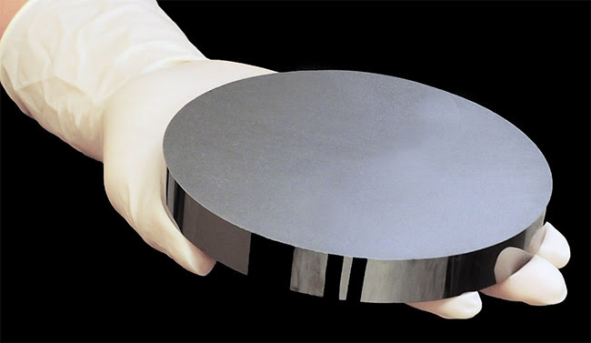
The first enabling technology for advancing the thermal imaging lens market was the development of chalcogenide materials. Chalcogenide glasses are amorphous materials containing sulfur (S), selenium (Se), and/or tellurium (Te) covalently bonded with elements such as germanium (Ge), arsenic (As), and antimony (Sb). These glasses transmit primarily in the midwave-infrared (MWIR) and LWIR wavebands, making them suitable for thermal imaging applications. Early development of these materials included a large variety of compositions to balance optical and mechanical properties, cost, reliability, and manufacturability. For instance, chalcogenides containing sulfur (branded as IRG 27 and AMTIR-6) tend to sacrifice transmission in the LWIR band for increased transmission in the NIR. Also, chalcogenides containing germanium (branded as BD2, GASIR1, IRG 22-25, AMTIR1, and AMTIR3) had early success in the industry but were subject to the high cost and temperature sensitivity of pure Ge relative to other available elements. For imaging applications, As2Se3 (branded as BD6, IRG 26, GASIR5, and IG6) has become the new industry standard for achieving optimal performance and manufacturability while maintaining minimum cost. Although all chalcogenides have been branded as athermal materials relative to the high temperature sensitivity of Ge, this particular composition has the best balance of properties for passively athermal optical assemblies (Figure 1).

Figure 1. Lens blank made from chalcogenide material. Courtesy of LightPath Technologies.
The second critical technology was precision glass molding (PGM). While the optical properties, availability, and low cost of chalcogenides provided a partial solution, it was the moldability of chalcogenide glass that uniquely qualified it for the high-volume demand of commercial IR applications.
Traditional crystalline materials, such as Ge, ZnS, and ZnSe, must individually undergo SPDT (single-point diamond turning) to prescription, while PGM is a high-throughput process that enables consistent production of high-accuracy lens form. In fact, contrary to popular belief, the precision and accuracy achieved in molding is often better in volume than that obtained through direct machining of lenses (i.e., SPDT).
For direct machining, high accuracy form may be achieved for low volumes, but the throughput required for higher volumes requires compromises in individually machined tolerances. However, the same high level of accuracy obtained in low volumes with direct turning can be attained in high volumes with molding. This is accomplished by investing extra time and care to dial in a single mold at the onset of production that will then be used to produce up to hundreds or thousands of near-exact replicas utilizing highly controlled and well-tuned molding stations.

Figure 2. Precision-molded, uncoated BD6 chalcogenide lens (left) next to a coated BD6 diamond-turned lens (right). Courtesy of LightPath Technologies.
While PGM has significant advantages, it is important to note that molding has its own set of limitations and design rules that warrant consideration, under select circumstances, of conventional SPDT techniques. The exact crossover point in manufacturability and cost-effectiveness between SPDT and molding is difficult to determine and must be assessed on a case-by-case basis for several reasons1. Continuous advancements and variations in process capabilities have caused outdated or misinterpreted information to
propagate through the industry and in recent literature. Additionally, much of this information has been spread by manufacturers with a particular bias toward one type of manufacturing over the other, for competitive reasons. Both of these manufacturing technologies, however, have advanced to the point where a balanced analysis of the benefits and limitations of each method (molding and SPDT), as well as the conditions under which each excels, is warranted (Figure 2).
Precision molding
Precision molding of aspheric lenses was first commercialized in the early 1980s2. In the decades since, this method of optical manufacturing has experienced mainstream acceptance across many vertical markets, from telecommunications to thermal imaging. PGM’s high repeatability, high surface quality, high volume capability, and low cost have all increased the popularity and commonality of this method of manufacture. Its excellent characteristics make it unique among optical manufacturing methods and serve as real differentiators.
PGM is an isothermal compression molding process. Before the molding process for a given lens begins, a set of mold tooling (upper and lower molds) must be fabricated, using a precise manufacturing technique such as SPDT.

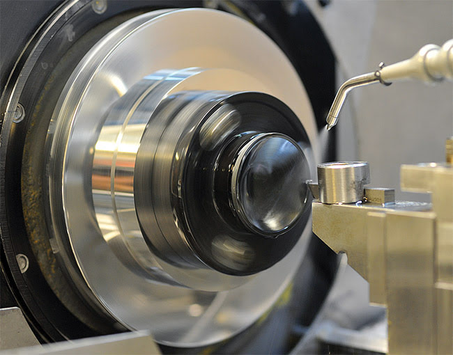
Figure 3. A BD6 chalcogenide lens undergoing precision single-point diamond turning (SPDT) processing. Courtesy of LightPath Technologies.
This mold tooling is manufactured to account for several factors in the replication process, including the desired surface of the finished lens, the thermal profile of the molding process, the properties of the moldable glass, and the material from which the molds are composed. The set of mold tooling is then installed in the molding machine, with a glass preform placed between the upper and lower molds.
A variety of glasses are moldable, but, principally, the glass must be amorphous. The molding machine is then purged with nitrogen (and sometimes under vacuum). From here, the glass preform and tooling are heated. Once the appropriate temperature is reached, pressure is applied, and then the mold is allowed to cool, resulting in a finished, stable lens.
What enables high repeatability is the controlled environment the glass is subjected to throughout the molding process. The ability to reuse the same mold tooling hundreds or even thousands of times helps reduce costs. Likewise, the ease of scaling the molding equipment helps enable parallel processing for high-throughput manufacturing. Mold tooling is manufactured using the same SPDT machines and processes, which means that lenses can be molded with the same high precision as lenses that are directly diamond turned, enabling tight tolerances in the finished molded lens.
Single-point diamond turning
The most common method for manufacturing aspheric optics for IR applications is SPDT, a deterministic material-removal process in which precision diamond tools are used on an ultraprecision lathe. A deterministic process is one in which the evolution of the process over time can be predicted exactly. The deterministic nature of SPDT enables very high yields and very high accuracies. Setup and process times are highly dependent on the required tolerances for the finished asphere. Almost all the IR ma-terials can be effectively diamond turned, whether they are crystals or glasses, such as the chalcogenides.
Table 1.
Comparison of the strengths and the limitations of diamond turning (DT) and precision glass molding (PGM).
| |
Diamond Turning |
Precision Glass Molding |
|
| Strengths |
• Has lower upfront costs.
• Scales easily to large sizes (up to ~100 to 200 mm).
• Uses crystalline or amorphous materials.
|
• Scales to high volume on acount of high throughput/capacity.
• Has lower costs with volume.
• Is capable of very small sizes (down to ~1 mm).
|
 |
| Limitations |
• Does not scale to high volume (capacity limited).
• Has higher production cost.
• Does not scale down to small sizes (i.e., <8 mm).
|
• Has higher upfront costs.
• Has limited manufacturability and yields for large sizes.
• Cannot mold crystalline
materials (Ge, ZnSe, etc.).
|
 |
SPDT is a mature technology; process times have been minimized through years of optimization. The efficient use of materials, extensive process development, and optimized metrology have resulted in a fully optimized process for the majority of the IR optical materials. When SPDT was still new, manufacturers had difficulties using it with chalcogenides because the material was unique, but nowadays lenses are easily diamond turned in large quantities (Figure 3).
SPDT, however, requires significant investment in equipment that is not readily scalable because it requires a machining process that repeats for each lens. Cycle times can be further minimized by reducing process and setup times at the expense of precision.
SPDT vs. PGM
The option to choose either method presents a significant opportunity for designers who select chalcogenide; regardless of size, shape, or quantity of lenses, they still have a cost effective solution. These factors simply drive the method of manufacturing, rather than becoming a constraint on the nominal optical design or performance.
PGM is commonly selected for higher-volume manufacturing and smaller lenses. The initial tooling cost for PGM chalcogenide aspheres typically makes very
small quantities cost-prohibitive, because the tooling cost needs to be amortized across the quantity. With larger quantities, the cost becomes trivial. Certain sizes and shapes are also more readily suitable for PGM3. The exact limits of size, shape, and quantity are interdependent, and they are evaluated on a case-by-case basis.
In order to compete with PGM in higher volumes, the SPDT process time must be minimized with feed rates and with tooling selection, which pushes the process to its limits in reducing cost. This cost reduction will, however, come at the expense of lower tolerances, because setup times need to be shorter, cutting speeds need to be faster, and material removal rates need to be greater. SPDT presents its biggest advantage for small-volume manufacturing (tens or hundreds of units) and for larger chalcogenide aspheres (several inches in diameter). The advantages of molding begin to diminish at larger sizes (~1-in. diameter) because equivalent high yields associated with SPDT are statistically difficult to achieve at these sizes (Table 1).
Chalcogenide aspheres provide many advantages in optical design for IR systems, and their application has revolutionized low-cost thermal imaging systems. Because of its amorphous nature, chalcogenide is unique among the common IR materials. This allows for a selection of manufacturing methods, including both direct machining as well as molding. In order to benefit from each technology in the effective use of chalcogenide aspheres, it is critical to rely on the expertise of well-established and reputable suppliers that have both capabilities.
Meet the authors
Jeremy Huddleston is the optical engineering manager at LightPath Technologies. He is responsible for optical design and testing at LightPath, and specializes in designing compact, low-cost lenses; email: [email protected].
Andrew Locke is the applications engineering manager at LightPath Technologies. He has a bachelor’s degree in optical engineering and has focused his career on technical customer-facing roles; email: [email protected].
Alan Symmons is the executive vice president of operations at LightPath Technologies. He is responsible for global operations and technology development at ISP Optics and LightPath; email: [email protected].
References
1. G. Cogburn et al. (May 3, 2010). Molding
aspheric lenses for low-cost production
versus diamond turned lenses. Proc SPIE,
Vol. 7660, Infrared Technology and
Applications XXXVI, https://doi.org/10.1117/12.850518.
2. A. Symmons and M. Schaub. (2016).
Field Guide to Molded Optics. Bellingham, Wash.: SPIE Press.
3. A. Symmons et al. (Sept. 27, 2016). Design
for manufacturability and optical performance trade-offs using precision glass molded aspheric lenses. Proc SPIE 9949, Polymer Optics and Molded Glass Optics: Design, Fabrication, and Materials IV,
2016, 994909, https://doi.org/10.1117/12.2238111.