Ceramic lasers offer design flexibility and pricing options that could change the way the world views solid-state lasers.
Jeffrey Wisdom, Michel Digonnet and Robert L. Byer, Stanford University
Ceramic lasers have the potential to dramatically reshape today’s marketplace for solid-state lasers. These still-evolving devices offer high output powers and low losses that are competitive with today’s best commercial solid-state lasers. Yet, because ceramics can be fabricated quickly, they can be much cheaper. Moreover, the physical and optical properties of ceramics can be tailored, providing the opportunity to engineer lasers with properties and costs that cannot be obtained in conventional lasers.
Transparent ceramic
Although commercial laser ceramics are only now beginning to emerge, transparent ceramics have been around since the 1950s. Early research was driven by nose cones for heat-seeking missiles, sodium streetlamps and fighter aircraft windows. The first commercialized transparent ceramic, called Lucalox,1 was introduced by General Electric Co. in the 1960s. This sapphire (alumina) ceramic is commonly used to form the bulbs of sodium streetlights because of its superior fracture strength and high thermal conductivity.
Today, the technology of alumina-based transparent ceramics has reached a high level of maturity. One example is ALON (aluminum oxynitride).2 Stronger, harder and lighter than glass, it is available in half-inch-thick sheets up to 20 by 32 inches. This versatile material has many applications, including military vehicles, forward-looking windows on planes and missiles, windows for bar-code scanners and scratch-resistant lenses.
An early ceramic laser was demonstrated in 1966 in dysprosium:CaF2. Recent ceramic lasers include the very promising Cr2+:ZnSe that operates in the 2.6-μm region.3 The quest to produce transparent oxide ceramics, such as YAG, has proved to be a difficult challenge, but recent progress has been astounding.
The development of laser-grade transparent ceramics has turned out to be a greater challenge, primarily because their performance requirements are significantly more stringent than those for window applications. In transparent ceramics, scattering is the greatest loss mechanism. It can originate from a number of sources, including pores, grain boundaries, compositional gradients within individual grains, as well as from optically anisotropic material phases and lattice imperfections, which can cause local index variations. Only in the last decade has the technology of transparent oxide ceramics matured to the point where scattering losses have been sufficiently reduced to achieve laser performance rivaling that of single crystals.
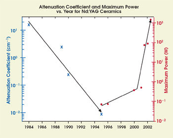
Figure 2. Much progress has been made in reducing scatter losses and increasing average power in ceramic Nd:YAG.
Dramatic progress has been made in reducing losses in transparent oxide ceramics (Figure 2). In 1995, Akio Ikesue reported an attenuation coefficient of 0.009 cm–1 4 and demonstrated the first ceramic oxide laser. This success was attributed to several technological improvements, particularly the use of a silica-based sintering aid to reduce the material porosity and, thus, the loss. Five years later, another group in Japan headed by Ken-ichi Ueda improved this efficiency figure to 53 percent with a ceramic manufacturing process that had taken more than a decade to refine and that had led to even lower losses.5
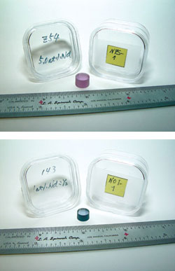
Figure 3. These research-size sintered ceramics with polished top surfaces are, above, 5 atomic percent Nd:YAG and, below, 1 atomic percent Nd:Y2O3. Courtesy of Akio Ikesue.
Since these initial demonstrations, the two groups have made remarkable progress. To date, ceramic Nd:YAG has reached 99.9999 percent theoretical density, 10 percent higher microhardness and five times higher fracture toughness than single-crystal YAG.6 It also has reached 58.5 percent laser slope efficiency (Figure 4)12 and has yielded up to 1.4 kW of output power (Figure 5).5 An Nd:YAG microchip (400 μm thick) laser with a doping level of 6.8 atomic percent pumped at the novel wavelength of 885 nm has demonstrated a 20 percent slope efficiency.7 Now ceramic Nd:YAG with doping levels up to 4 atomic percent is available in the US through Baikowski International, a corporation partnered with the patent-holding Konoshima Chemical Co. of Japan.
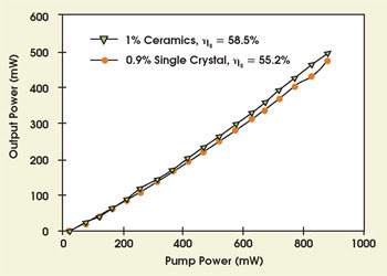
Figure 4. In this low-power comparison of ceramic and single-crystal Nd:YAG, the former has reached 58.5 percent laser slope efficiency.
Besides Nd:YAG, several other ceramic systems have shown laser oscillation, including Yb:YAG, Nd:YSAG, Nd:Y2O3 and Yb:Sc2O3.8-11 The high thermal conductivity of Y2O3, twice that of YAG, and broad emission spectra in Nd:YSAG and Yb:Sc2O3 make these materials attractive as laser gain hosts. Previously, the growth of Y2O3 was difficult because of its very high melting temperature of ~2430 °C. Ceramic processing occurs below the melting temperature and allows the fabrication of high-optical-quality materials in sizes that are attractive for commercialization.
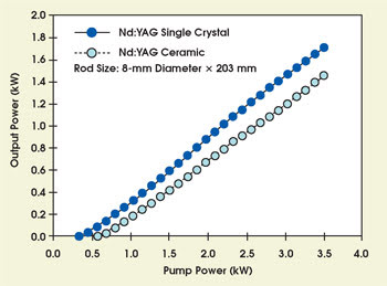
Figure 5. In this output power vs. pump power data for Nd:YAG ceramic and single-crystal samples, the ceramic has yielded 1.4 kW of output power.
Until the advent of laser ceramics, most crystal laser hosts could be fabricated only by crystal-growth methods such as the Czochralski method. These techniques rely on melting the material and using a seed crystal to crystallize the melted material during cooling. The Czochralski method, the most common commercial growth technique for the production of Nd:YAG, produces crystal boules by pulling seed crystals from a melt in an iridium crucible. The temperature must be maintained above YAG’s melting temperature (1960 °C).
The production of a crystal boule can require two weeks or longer. During this time, impurities from the crucible can be introduced into the melt and then into the crystal. Further, it is exceedingly challenging to prepare single-crystal boules larger than 6 inches in diameter by the Czochralski growth method without excess stress or crystal fracture. For example, in Nd:YAG, the crystal growth process induces a highly stressed core region that runs through the center of the boule. Residual stresses in the boule introduce undesirable wavefront distortion and limit the size of the fabricated crystal.
Ceramic processing offers numerous advantages over Czochralski growth. Ceramics are produced by forming high-purity YAG nanopowder into the desired shape, then sintering in a vacuum. Typically, the process takes only 24 hours. In addition, and quite importantly, ceramics can be manufactured in sizes limited only by the size of the processing equipment. This benefit is similar to that of laser glasses, but with greatly increased thermal conductivity and a greater resistance to thermal failure for the ceramic relative to glass. The availability of large laser gain media with both high thermal conductivity and optical quality is expected to have a dramatic impact on high-average-power laser systems as well as on future high-energy-storage laser systems.
Ceramics also can sustain doping levels much higher than melt-grown crystals, which is useful in microchip laser applications. The small sizes of the crystal grains allow stress induced by high Nd-doping levels to be relieved in short distances at grain boundaries. Also, the dopant percentages in the precursor materials remain in the final ceramic piece, a strong advantage compared with Czochralski growth, where the larger dopant ions are often rejected at the crystal-melt interface, resulting in a lower doping percentage in the crystal than in the melt.
Ceramics also can be engineered to exhibit a variety of interesting dopant profiles. Progress in this direction includes the demonstration, in 2000, of a novel step-function doping profile using a circular disk of Yb:YAG. The center of the disk was doped with 25 atomic percent Yb:YAG, and the surrounding material was undoped, a configuration that allows efficient side-coupling of pump radiation. Ceramic materials with step-function doping profiles are available through Baikowski.
It also may be possible to create composite gain media, namely materials that contain two or more functional components, such as an Nd:YAG section combined with a Cr4+:YAG section that acts as a passive Q-switch. Composite materials would eliminate the need for separate diffusion bonding steps during the manufacture of specialized laser crystals, thus drastically reducing their cost and manufacturing time. The development of fast and cost-effective methods for modifying doping profiles and integrating components is a revolutionary concept in the field of lasers. Once mastered, it is expected to offer unmatched flexibility in the design of laser systems.
The impact of ceramics
The combination of design flexibility and low cost will allow laser gain media to be engineered cost-effectively. Research at Stanford University in California is seeking to capitalize on these advantages in power-scaling solid-state lasers, both in CW and mode-locked regimes, by reducing laser absorption losses and finding crystal hosts with high thermal conductivity and efficient small-quantum-defect pump bands.
There are many applications for this technology, from stable high-power lasers for gravitational wave detection to industrial needs to very high average power lasers for military applications. Breakthroughs also have been made in the flexibility of ceramics to accommodate high average powers:
• Thermal conductivity and absorption length. In the area of microchip lasers, pump absorption must be maximized to reduce crystal size. Nd:YVO4, which has commonly been employed in such applications, has been preferable to Nd:YAG because it has a six times higher absorption cross section at 808 nm. However, Nd:YVO4 has poor thermal conductivity — less than half YAG’s — which is a major hurdle when scaling to higher powers. Ceramic processing now enables doping Nd:YAG to levels greater than 6 atomic percent, where its absorption length is comparable to that of Nd:YVO4. Given its significant heat conduction advantage, ceramic Nd:YAG appears to be the material of choice.
• New pump bands for a lower quantum defect. By increasing the doping level of Nd:YAG, it also becomes possible to pump neodymium bands that normally do not have a high enough absorption coefficient for efficient pumping. This was recently demonstrated with the 885-nm transition of Nd:YAG. Pumping at 885 nm is advantageous because it reduces the quantum defect by 30 percent compared with conventional pumping at 808 nm, thereby improving overall efficiency and reducing the thermal load. A microchip laser pumped at 885 nm has demonstrated a slope efficiency of 51 percent compared with 47 percent when pumping at 808 nm.7 Such improvements should help scale solid-state lasers to higher powers.
• Shorter mode-locked pulses. Interest is growing in mode-locked lasers offering picosecond pulses with high average powers for micromachining applications. To generate short pulses, mode-locked oscillators require a large gain bandwidth (emission spectrum), while high average powers require high thermal conductivity and diode pumping. Nd:YAG is not suitable for this application because its emission spectrum is fairly narrow and limits the pulse width to ~5 ps.
In Nd:YSAG (Nd:Y3ScxAl(5-x)O12), a variant of YAG, the presence of scandium distorts the unit cell, which creates two chemically distinct locations for neodymium to replace yttrium. The result is an emission spectrum more than five times wider than that of Nd:YAG, high pump absorption and good thermal conductivity. This material has enough bandwidth to support subpicosecond pulses, making it a good candidate for a power-scalable diode-pumped mode-locked laser. Nd:YSAG is difficult to grow as a single crystal, but high-quality ceramic material has been fabricated recently, resulting in a laser demonstration with a slope efficiency of 30 percent.9
Yb:YAG is another attractive material for high-average-power mode-locked lasers. It offers a large gain bandwidth and has already demonstrated more than 50 W of average output power. Yb:Sc2O3 might be an even better candidate for this application. Its emission spectrum is twice as broad as that of Yb:YAG, offering pulses two times shorter, and it has a lower transparency threshold, a higher saturation intensity and almost twice the absorption linewidth for efficient pumping. Its high melting temperature (~2430 °C) made it very difficult to produce Yb:Sc2O3 samples of large size and high quality using crystal-growth methods. Recently, J. Lu et al have developed ceramic Yb:Sc2O3.11 Although this process requires very expensive precursor materials, it is an interesting demonstration of the potential of ceramics in the area of high-melting-point materials.
A promising future
Ceramic technology stands out from current crystal-growth techniques because it is the only fabrication method that combines composite device structures, new material possibilities, size scaling and cost-effective fabrication. The future may herald ceramic gain media with extremely small quantum defects (less than 5 percent), which could have a great impact on power scaling. With advances coming at an accelerated pace, some of these developments may soon become a reality.
Meet the authors
Jeffrey Wisdom is a PhD candidate in the applied physics department at Stanford University in California.
Michel Digonnet is senior research engineer and Robert L. Byer is professor of applied physics at Stanford.
References
1. J.E. Burke (June 1996). MRS BULLETIN, p. 61.
2. T.M. Hartnett et al (1997). Window and dome technologies and materials V. Proceedings of SPIE, Vol. 3060, pp. 284-295.
3. S.A. Payne et al (1997). IEEE J. on Sel. Top. QUANT. ELEC., 3, pp. 71-81.
4. A. Ikesue (2002). OPTICAL MATERIALS, 19, pp. 183-187.
5. J. Lu et al (2002). JOURNAL OF ALLOYS AND COMPOUNDS, 341, pp. 220-225.
6. A. Kaminski et al (2003). CRYSTALLOGRAPHY REPORTS, 48, pp. 515-519.
7. V. Lupei et al (2001). APPLIED PHYSICS, B, 73, pp. 757-762.
8. K. Takaichi et al (2003). PHYS. STAT. SOL., 200, pp. R5-R7.
9. Y. Sato et al (2003). The spectroscopic properties and laser characteristics of polycrystalline Nd:Y3ScxAl(5-x)O12 laser media. OSA Trends in Optics and Photonics, Vol. 83, Advanced Solid State Photonics, pp. 444-450.
10. J. Lu et al (2001). JAPANESE JOURNAL OF APPLIED PHYSICS, 40, pp. L1277-L1279.
11. J. Lu et al (2003). APPLIED PHYSICS LETTERS, 83, pp. 1101-1103.
12. J. Lu et al (2001). JAPANESE JOURNAL OF APPLIED PHYSICS, 40, pp. L552-L554.
Ceramics Defined
Optically transparent ceramics consist of small crystalline grains sintered to form bulk material. Sintering is the forming of bulk material from smaller particles by heating the material to just below its melting temperature to facilitate the growth of crystallites in the 10- to 30-μm range.
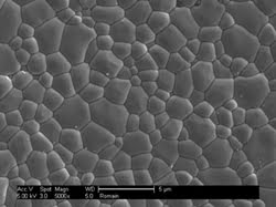
Figure 1. This undoped and unpolished YAG ceramic, imaged by scanning electron microscopy, was fabricated at Stanford University. Courtesy of Romain Gaume.
As a result, laser ceramics are a mosaic of small, closely packed crystalline grains (Figure 1). Yet despite their polycrystalline nature, properly prepared ceramics exhibit transparency and thermal mechanical properties very close to those of single crystals. All of the properties critical to laser performance — in particular, propagation loss, thermal conductivity, dopant absorption and emission characteristics, and optical isotropy — are similar to those of single-crystal laser hosts.
In fact, the primary difference between an ideal ceramic and a single crystal is the existence of a unique material state at the grain boundaries that results in no appreciable scattering loss or mechanical weakness. Given the small effective volume of this layer compared with crystalline grain volume, typically less than 0.3 percent of dopant ions experience environments that would lead to inhomogeneous broadening.