Search
Menu
CMC Electronics - Advanced Low-Noise 2024 LB

Big research on tiny technologies

Facebook X LinkedIn Email
Anne L. Fischer, Senior Editor, [email protected]

IMEC is one busy research center. Headquartered in Leuven, Belgium, the independent research and development center focuses on nanoelectronics and nanotechnology, partnering with companies, universities and other research institutes. One example of the collaborative approach can be seen in the development of technologies and devices for the body and mind.

The Human++ research program, which is operated through IMEC and the Holst Centre in Eindhoven, the Netherlands, focuses on the development of miniaturized devices and technologies that attach to the body to determine a diagnosis or provide feedback on the status of various therapies. Many partners take part in the research. One example is Terepac of Waterloo, Ontario, Canada, which packages the electronics that go into wireless electro-cardiogram (ECG) systems.

Terepac brings to the program its expertise in the photochemical printing process, in which thinned silicon dies and passive components are placed on flexible substrates that go into a wireless ECG patch. As with other partnerships within the center, the relationship between IMEC and Terepac is mutually beneficial: IMEC benefits from Terepac’s package assembly capabilities, and Terepac has the advantage of being able to test its technology in the final stages of production and application.

Advancing the smart grid

Lowering costs and increasing the performance of power devices such as smart meters, switches, sensors and actuators – all of which play a role in alternative energy – are other areas of focus. Gallium nitride (GaN) devices have shown promise for use on the electrical grid of the future, but making them cost-effectively means producing very large GaN wafers. As a result of collaboration with Aixtron of Crystal Lake, Ill., IMEC launched an industrial affiliation program, with a goal of working toward lowering the cost of GaN technology by using large-diameter GaN-on-silicon. Potential applications include high-power switching in solar converters, motor drives and hybrid electric vehicles.
Meadowlark Optics - Wave Plates 6/24 MR 2024

Greenlight1.jpg
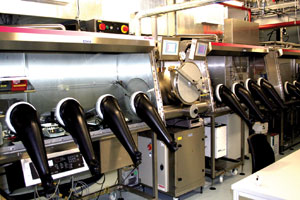
IMEC cooperates with the photovoltaic industry on research and development of highly efficient thin-film crystalline-silicon solar cells and advanced photovoltaic technology, such as organic solar cells and solar concentrators with photovoltaic stacks.

Aixtron provides the equipment that makes GaN-on-silicon wafers for the solid-state lighting market, among others. With this equipment, researchers at IMEC demonstrated crack-free GaN growth on 200-mm wafers. According to Frank Schulte, vice president of Aixtron Europe, IMEC is a “kind of showroom,” where the equipment is in front of a lot of end users, who he said are all potential customers. The benefit to IMEC is the potential development of high-voltage, low-loss, high-power switching devices based on large-diameter GaN-on-silicon technology.

By sharing costs and resources, partners bring in products and technology that become part of the research and development process, and cross-fertilization is the result. While IMEC is headquartered in Belgium, its offices in China, the Netherlands, Japan, Taiwan and the US afford the center the opportunity to have an impact on the technologies of our global future.

Published: December 2009
Glossary
actuator
An actuator is a mechanical or electromechanical device that is responsible for moving or controlling a mechanism or system. It converts various forms of energy (such as electrical, hydraulic, pneumatic, or thermal energy) into mechanical motion. Actuators are widely used in various industries and applications where precise control and movement are required. Functionality: Actuators are used to initiate or control motion by converting energy into mechanical force or displacement. They can...
gallium nitride
Gallium nitride (GaN) is a compound made up of gallium (Ga) and nitrogen (N). It is a wide-bandgap semiconductor material that exhibits unique electrical and optical properties. Gallium nitride is widely used in the production of various electronic and optoelectronic devices, including light-emitting diodes (LEDs), laser diodes, power electronics, and high-frequency communication devices. Key points about gallium nitride (GaN): Chemical composition: Gallium nitride is a binary compound...
nanotechnology
The use of atoms, molecules and molecular-scale structures to enhance existing technology and develop new materials and devices. The goal of this technology is to manipulate atomic and molecular particles to create devices that are thousands of times smaller and faster than those of the current microtechnologies.
photochemical
The term photochemical pertains to chemical processes or reactions that are initiated or influenced by the absorption of light. Photochemical reactions involve the interaction of light, often in the form of ultraviolet or visible radiation, with molecules, leading to changes in their chemical structure or properties. These reactions are distinct from thermal or non-light-induced chemical reactions. Key characteristics of photochemical reactions include: Light absorption: Photochemical...
sensor
1. A generic term for detector. 2. A complete optical/mechanical/electronic system that contains some form of radiation detector.
substrate
A substrate refers to a material or surface upon which another material or process is applied or deposited. In various fields, such as electronics, biology, chemistry, and manufacturing, the term "substrate" is used with specific contexts, but the fundamental definition remains consistent: it is the underlying material or surface that provides a foundation for subsequent processes or applications. Here are some examples of how a substrate is used in different fields: Electronics: In...
actuatorAixtronAnne L. FischerBelgiumConsumerCrystal LakeCrystalline SiliconECGEindhovenelectrocardiogramenergyFrank Schultegallium nitrideGaNGaN-on-SiglobalGreenLightgridHolst CentreHuman++IllinoisIMECindustrialJapanLeuvenmanufacturingnanoelectronicsnanotechnologyNetherlandsOntarioorganic solarphotochemicalphotovoltaic stacksphotovoltaicsprintingResearch & TechnologysensorSensors & Detectorssiliconsolalr concentratorssolarsolid-state lightingsubstrateTaiwanTerepacthin-filmUSWaterloo

We use cookies to improve user experience and analyze our website traffic as stated in our Privacy Policy. By using this website, you agree to the use of cookies unless you have disabled them.