Today and Tomorrow
Brian D. Potteiger, Steven R. Solometo and William K. Fritz
Manufacturers of optoelectronic components must automate to meet the needs of the telecommunications
industry. The semiconductor experience is a useful but imperfect model.
The financial situation confronting the optical networking industry is placing new demands
on the companies that supply it with advanced optoelectronic components. Because
of the recent slowdown in spending, carriers are looking for ways to maximize the
value of their expenditures on network equipment. Nevertheless, purchases will still
be required to maintain the growth of the network.
Service providers must focus on three areas when
considering equipment purchases: reducing capital expenditures, trimming operational
expenses and creating means of generating revenue. Accordingly, component manufacturers
must provide highly integrated products that are smaller, faster and cheaper. To
increase the value-added benefits of these components and to meet the ever more
exacting performance criteria, critical processes must be mechanized or automated.
Optoelectronic component manufacturing,
however, still is rooted in the largely manual or mechanized processes that prevailed
in the research-and-development and start-up phases of the industry’s evolution.
To be sure, there are islands of automation in photonics today, and that’s
a good sign. But it is only the first step in a long journey.

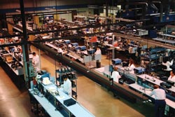
There are islands of automation in photonics today, but optoelectronics
manufacturing still is rooted in the hands-on processes of the research-and-development
and start-up phases of its evolution.
The increasing demand for optoelectronic
devices that require very precise component placement — approximately 5 to
25 μm — and that require the integration of multiple functions in the
same package has forced the industry to move beyond manual assembly. With the additional
requirement of higher levels of functionality in smaller packages, the need for
automation is even more important.
Different approach needed
The automated manufacturing of integrated circuits
has been around for decades. Although it offers a relevant model for optoelectronic
automation, there are significant differences.

The manufacture of integrated circuits is a useful — but imperfect
— model for the automation of optoelectronic components. Optical components
feature unique and critical alignment parameters.
Besides their lower volumes, optoelectronic
components are still characterized by the assembly of discrete parts, such as laser
chips, lenses, integrated circuits, isolating optics and fiber pigtails. Moreover,
optical components feature unique and critical alignment parameters. For example,
coupling the light from laser to fiber has a tolerance on the order of several microns
in multiple axes, a significant challenge for an operator to perform manually in
a timely and repeatable fashion. And the process must be sufficiently robust to
ensure minimal “shift” after assembly.
Emerging technologies are placing an
even greater emphasis on precision. For example, microelectromechanical systems
(MEMS) technology has shifted the critical tolerances into the submicron range.
Given the size and cost of MEMS arrays, there is a premium on getting the job done
right the first time.
Lastly, unlike semiconductor manufacturers,
those in optoelectronics do not enjoy the benefit of the years of collaboration
with equipment makers that led to development of high-quality, off-the-shelf production,
assembly and test gear. Optoelectronics manufacturers either developed their own
solutions — at considerable risk and expense — or tried to increase
the mechanization of existing operations.
Developing an automation platform from
the ground up offers distinct advantages over this piecemeal approach. Agere Systems,
for example, has adopted a comprehensive strategy in which the assembly, packaging
and testing of optical subassemblies is automated to accommodate high-volume production.
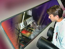
Each piece of equipment features an
enclosure to ensure a cleanroom environment throughout the process. Engineering,
development and production staff, along with supervisors, share space on the shop
floor, creating a spirit of close collaboration as well as rapid resolution of issues.
This approach reduces processing steps by half and improves manufacturing intervals
by a factor of five, while increasing product reliability and quality.
Building-block approach
System manufacturers are looking for subsystems
that integrate multiple functions to increase time-to-market and to improve operating
expenses. A building-block approach to automation addresses this need by offering
the flexibility to incorporate many critical functions in the same transmitter package.
For example, laser driver integrated
circuits can be combined with 10-Gb/s electroabsorptive-modulated lasers through
automation to improve radio-frequency performance and to increase the transmission
distance. In addition, tunable laser transmitters can include lockers for wavelength
stabilization, RAM modules that give customers look-up tables to set the laser output
power and drive current, and an easy-to-use digital interface for customer programming.
Agere’s optical subassembly,
also known as a silicon optical bench, is a standardized carrier for laser chips,
lenses and fiber couplings for a variety of products, including 1300- and 1550-nm
lasers and dense wavelength division multiplexer and electroabsorptive-modulated
laser sources. The 2.5 x 3.5-mm silicon carrier serves to build hundreds of subassemblies
with the flexibility to accommodate laser chips of different wavelength and power
output. We use a butterfly optical package, standardized on a single footprint,
to facilitate automated handling and the associated assembly and test processes.
The optical subassembly and other components
are bonded to a ceramic substrate and put into the package body. The electrical
interconnects, or wire bonds, are made between the subassembly and the package,
which then is hermetically sealed with a lid. A fiber pigtail is attached to the
package by laser welding. Finally, the completed package assembly is tested on automated
equipment, with no human intervention or handling. The results are sent to a database
with other test results, providing a complete, detailed record for all devices processed
in the facility.
Material handling is a critical and
often overlooked element of automation. Because of developments in the semiconductor
industry, most aspects of material handling, along with the equipment to transport
the components, are commercially available.
The optical subassemblies are carried,
processed and tested in a 50-position waffle pack. Five packages are carried and
processed in a metal boat, and 10 boats are transported in each magazine. For testing,
an internally designed, injection-molded subboat carries the package and fiber with
a test plug — one completed package with fiber per subboat and two subboats
per metal boat. The subboat is attached to a metal boat and automatically presented
to the testing equipment.

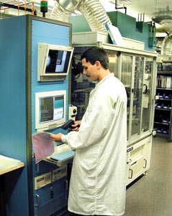
Most automated material-handling systems required by optoelectronics manufacturers are
commercially available. Here, a metal boat holds five 14-pin butterfly packages
that are hermetically seam-sealed using automated lid-attach equipment.
Accuracy, repeatability
The subboat accurately and repeatably presents
the package and the plug so the laser power, wavelength and other parameters required
by the customer can be tested. These tests are performed at ambient temperature
as well as over temperature ranges. Because the subboat was designed to be low in
cost (less than $1), it is removed from the metal boat and placed directly into
the shipping container for delivery to the customer.
Data management is another key element.
Data must be available to customers as requested to facilitate the deployment of
the components in their systems. The large number of product codes that may be manufactured
on the same line compounds the complexity of the task.

Data management is an essential aspect of automation. A technician
scans a bar code to track the lot of optical subassemblies during the assembly process.
Databases, while costly and complex
to design and implement, also enable the control and tracking of a product’s
performance from design through assembly, testing and shipping. Performance data
gives the manufacturer the means to analyze and correct problems with materials
and processes, assuring ever-increasing quality to match or exceed the customers’
rising expectations. The manufacturer also can use the data to proactively anticipate
process and product problems and to make corrections prior to manufacturing a product
that does not conform to specifications.
Automating for tomorrow
Moreover, database systems can be used to track
the performance and output of individual workstations and machinery, thereby providing
opportunities for better use of capital equipment and for increased productivity.
And automated information systems help to manage inventories and to improve delivery.
A holistic approach to automation can
prove extremely successful for high-volume manufacturing. However, with so many
products and customer requirements in the optoelectronics industry, across-the-board
automation often is not an option. Each manufacturer must perform a comparative
cost/benefit analysis of the manual, mechanized and automated options, taking into
account the precision requirements of the optical and electrical design, the necessary
volume, the cost target, the yield objectives, the load rates, and the availability
and cost of labor. In some cases, the manufacturer may choose to have subassemblies
carried and loaded into machines manually but to have automated machinery handle
repetitive tasks, such as the placement and soldering of components.
Some optoelectronics manufacturers
have made remarkable strides in designing the equipment to automate specific processes,
but the industry can’t go it alone. It is imperative to seek out equipment
suppliers who can provide reliable, economical and off-the-shelf automation solutions.
The challenge is to develop pick-and-place equipment that can handle components
of irregular shapes and sizes, a variety of materials and varying alignment features,
and that can perform assembly and test operations, maintaining tolerances in the
range of 5 to 25 μm in as many as six axes. Equipment exists that addresses
these requirements individually; equipment that addresses all does not.
As the state of the art in optoelectronic
systems reaches — and surpasses — 40 Gb/s, it will be necessary to integrate
more components and functions in optical packages. For example, the need to detect
and monitor electrical signals at 40 Gb/s is extremely important because slight
variations in the length of the electrical path can severely affect the sensitivity
of a receiver. Using automated processes, high-speed waveguide detectors and distributed
amplifiers can be integrated inside 40-Gb/s receiver packages, giving customers
better control of these critical interfaces and improving performance.
Looking ahead, separate operations,
such as flip-chip bonding, must be unified in a seamless process. Industry standards
for material handling of optoelectronic components such as fiber, optical and radio-frequency
connectors, packages and other subassemblies must be developed and established.
This is common in the semiconductor industry; it must become common in optoelectronics.
Product design challenges also must
be overcome to increase the use and value of automation in the industry. One is
the development of optical designs that will meet customer requirements and that
can accommodate relaxed assembly tolerances. Along the same lines is the ability
to design optical components that facilitate active alignment with relaxed subassembly
tolerances.
Finally, most optoelectronic components
today are assembled passively — they are picked and placed but not electrically
or optically biased. The ability to passively assemble the majority of components
with reduced tolerances and to perform the active alignment of an optical element
would have a significant impact on yield and on product and process characterization.
Meet the authors
Brian D. Potteiger is technical manager of manufacturing
technology, equipment, software and automation at Agere Systems in Allentown, Pa.
He holds a BS in mechanical engineering and an MS in engineering science from Pennsylvania
State University in University Park.
Steven R. Solometo is senior manager
of automation, robotics and software applications at Agere. He holds a BS and an
MS in computer science from Penn State and from Villanova University, respectively.
William K. Fritz is director of manufacturing
technology at Agere. He holds a BS and an MS in electrical engineering from Penn
State and from Clemson University, respectively.