As photonic devices diminish in size to chip-scale solutions, they promise to expand their value and reach as biomedical and analytical tools. But with miniaturization comes new challenges.
MICHAEL EISENSTEIN, CONTRIBUTING EDITOR
Early in his career, Benjamin Miller was focused on drug discovery and strategies for studying how potential medicines bind to their target proteins. There was only one problem: “All of the technology that was available for doing that was terrible,” said Miller, a biochemist and engineer at the University of Rochester. “So, we decided to start working to fix the problem.”
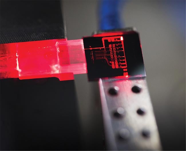
Integrated photonics are enabling ever-smaller biosensing chips that promise to offer fast, affordable, and highly sensitive analytical tools for point-of-care applications. Courtesy of LioniX International.
The solution that he ultimately identified involved leveraging photonic integrated circuits (PICs) to construct miniaturized sensors that can monitor
analytes using various light-based analytical techniques. “Because you’re using photons, you can take advantage of spectral properties of molecules,” Miller said. This makes it possible to achieve remarkably sensitive detection of targets without the molecular labeling steps that are commonplace in many bioassays. And just as relentless progress in the semiconductor industry has enabled astonishing miniaturization of virtually every electronic device, advancements in PIC technology could likewise fuel the development of tiny — or even wearable — devices that perform analyses currently reserved for bulky instruments.
Early advancements in the PIC-sensor space have already demonstrated some
of the possibilities. Companies such as Surfix Diagnostics and Delta Diagnostics are working on photonic sensors that quantitatively detect multiple health-related biomarkers in parallel, such as molecular signatures of cancer or other diseases. Miller’s group is developing sensors that can be used to monitor the physiological status of tissue-on-a-chip systems, which are simplified in vitro models of human organs that have proved to be powerful for studying disease
pathology and testing drugs.
There are numerous non-biomedical
applications as well. For example, Spectrik and Deloq are developing PIC-based sensors that can track emissions of environmentally damaging gases, such as ammonia and methane, while Manti-Spectra is building PIC devices suitable for the spectroscopic analysis of materials ranging from agricultural products to contraband narcotics.
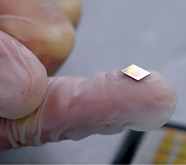
Companies such as Qurin Diagnostics are developing diagnostic chips that can quantitatively detect multiple health-related biomarkers in parallel, such as molecular signatures of cancer and other diseases. Courtesy of LioniX International.
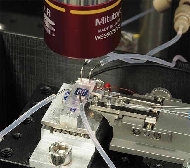
Biochemist Benjamin Miller’s lab at the University of Rochester is coupling photonic ring resonator-based sensors to organ chips — simplified in vitro models of human organs that are proving to be powerful tools for analytical studies into disease pathology and drug development. Courtesy of Benjamin Miller Lab.
Despite these developments, the field is still waiting to take off. Only a handful of devices have reached the market. Developers are still grappling with the challenges of designing and manufacturing PIC sensors at scale, and identifying use cases where these systems offer a decisive advantage over more mature electronics-based technologies.
“Basically, the whole market is looking for one thing: a killer application,” said Hans Dijk, business development manager at Surfix.
Everything is illuminated
Kaylee Hakkel, COO at MantiSpectra, wants to manage expectations about what PICs can and cannot do. “Photonics is never going to replace electronics like some people say,” she said. “But it will open up so many new applications.” This is due to the diverse array of sensing modalities that are available or exclusive to photonics-based platforms.
Many biochemical detection assays depend on antibodies that bind strongly to specific biomolecular targets, but these assays often require dyes or other chemical labels to generate a readout. PIC-based sensors can overcome these limitations by rapidly quantifying how antibody-target binding events influence the behavior of light. This generally entails physically tethering antibodies or other target-binding molecules to the chip surface and using a detector to monitor the behavior of an incoming light beam when the
sensor is exposed to a clinical sample.
One iteration of this approach, commercialized by medical diagnostics companies such as SiPhox and Genalyte, couples antibodies to circular structures called microring resonators. The binding of the antibody to its target produces a change in the refractive index of the solution adjacent to the resonator, enabling sensitive and rapid detection of binding events.
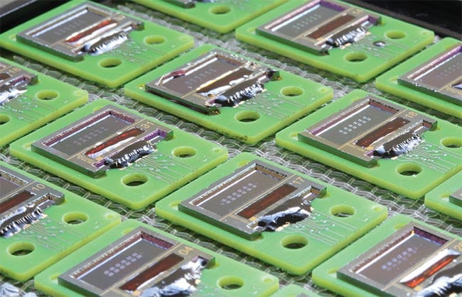
Biochemists, PIC designers, and foundries are working together to overcome the challenges of designing and manufacturing PIC biosensors at scale. Courtesy of LioniX International.
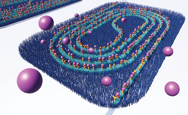
Surfix BV, Qurin Diagnostics, and LioniX International have developed a chip-based system that uses refractive index sensing of biomolecular analytes based on an asymmetric Mach-Zehnder Interferometer (aMZI). This artist’s impression of the biochip shows a functionalized surface of the aMZI transducer with biorecognition agents applied on the waveguide surface. The receptors, appearing as the yellow Y-shaped stems, are attached to a coated waveguide (cyan) and latch on to virus particles (purple spheres). Courtesy of Surfix BV.
Surfix is pursuing a different approach based on Mach-Zehnder interferometry, which monitors the phase shift of light at a sensor element modified with an antibody or another target-recognition molecule, and compares that shift to the signal of an unmodified reference sensor element. Interferometric and resonator
approaches can both be multiplexed to track several targets at once, but interferometry can also confer certain advantages in terms of sensitivity.
Surfix is currently focused on detecting DNA and protein signatures of cancer in the context of minimally invasive liquid biopsies performed on samples such as blood or urine. “We’re aiming for sensitivities that go below the picograms-per-milliliter level,” Dijk said. Such sensitivity is essential, because liquid biopsies are especially valuable for detecting scarce signals from very early-stage cancer or small numbers of tumor cells that survive initial treatment.
Infrared (IR) spectroscopy is another popular analytical method. Rockley Photonics has developed a wearable wristband that monitors changes in infrared absorbance in the bloodstream and renders a measurement of blood pressure and other physiological parameters. IR spectroscopy is also a powerful method for characterizing chemical compounds and mixtures based on their distinctive absorbance spectra, and MantiSpectra is using this approach in a sensor platform that can evaluate diverse solids and liquids in a nondestructive, contact-free fashion. “We can detect fat and protein content in milk, for example,” Hakkel said. “Or for recycling, you can use it for different types of plastics.”
Researchers are also miniaturizing other powerful analytical techniques. For example, Miller is working on chip-based Raman spectroscopy, a profiling method that discerns the unique vibrational characteristics of different molecular analytes. “It’s really great for small molecules that you might want to detect in a blood sample, like creatinine, which is a marker of kidney disease, or for a chemical sensor to detect things like fertilizer or sarin gas or what have you,” he said. Axithra, a newly formed spinoff of Belgian PIC foundry IMEC, is focused on developing Raman-based chips for monitoring drug concentrations in the bloodstream.
Some assembly required
Shrinking sophisticated sensor systems down to chip-scale can be tricky. On one hand, PIC design and manufacturing is not entirely new territory. “By and large, integrated photonics uses well-established processes from the semiconductor industry; they’re not the same, but similar,” said Carol de Vries, CTO of PhotonDelta, a Dutch public-private partnership focused on advancing PIC commercialization. And there are mature applications of PIC technology, most notably in telecommunications and computing.
But PIC-based sensors bring distinct challenges to the table. First, one must consider the material platform being employed. Conventional silicon photonics chips do not exhibit optimal optical properties for a lot of sensing applications. Many sensor developers opt to use silicon nitride (SiN)-based waveguides as a more robust alternative. “Silicon fundamentally suffers from losses once you increase your power, while silicon nitride doesn’t because the bandgap is much larger,” said Columbia University photonics researcher Michal Lipson. “Silicon nitride has been shown to have extremely low losses, even at low power.”
Unfortunately, SiN is only suitable for passive transmission of light and cannot be used to fabricate light sources and detectors. Indium phosphide (InP) is a standard material for producing such active photonic components; even some sensors, such as those produced by MantiSpectra, can be entirely fabricated from InP.
According to Hakkel, silicon-based elements also do not perform as well at the IR wavelengths used for the company’s preferred analytical applications. With InP-based devices, she said, “We cover the full range from 850 to 1700 nm.” But the visible-to-near IR range, where SiN excels, is optimal for many biomedical use cases, and this means that sensor developers need a way to efficiently relay light into and out of their chips.
If miniaturization or a wearable device such as Rockley’s biosensor bracelet is the goal, then direct coupling of SiN- and InP-based components is generally required. Typically, this is achieved via hybrid integration, which entails the precise coupling of individual chips within the sensor device either via lateral edge-coupling or vertical flip-chip assembly. Both approaches are now reasonably straightforward and scalable, said Sadoon Al-Obaidi, marketing and communications director at Dutch PIC foundry
LioniX. “We have already developed all the solutions for getting the gain chip and the silicon nitride chip all put together and into a device that maintains the performance,” he said.
There is also considerable interest in heterogeneous integration approaches that sequentially fabricate active and passive elements onto the same wafer. These are considerably less mature, but de Vries points out that heterogeneous integration could one day prove to be more economical for producing larger-scale batches of hundreds of thousands or more PIC-based devices.

To some extent, integrated photonic sensors are helping to miniaturize biosensors and analytical tools are able to take advantage of cost-efficient semiconductor fabrication methods. But the active and passive photonic components involved often require very different materials, fabrication techniques, and packaging than conventional silicon electronics. Courtesy of LioniX International.
There are also arguments for avoiding chip-based active elements and working
with external lasers and detectors within a separate reader device. “That’s a big discussion in the industry,” said COO and cofounder of PIC packaging foundry PHIX, Joost van Kerkhof. He said that external optical components can also introduce design complexity. “What drives the cost of an off-chip light source is not so much the light source, but more the coupling of the light into the chip,” said van Kerkhof, and these design considerations can drive the cost of a reader system into thousands of dollars. On the other hand, taking these elements off-chip makes the chips themselves cheaper, or even disposable, and simpler to produce. This can be a critical consideration if the goal is low-cost diagnostic testing, and such a model is favored by companies such as Surfix and SiPhox.
Biochemical sensing can also be a thorny challenge, often requiring the coupling of microfluidic components to channel blood or other specimens to the detection site. Dijk said that Surfix has grappled with developing bonding strategies for coupling its microfluidic cartridge to the PIC to minimize the risk of leaching and sample contamination by the chosen adhesive. Such sensors also require special treatments that protect the sensor surface against fouling by biomolecules in the sample and that enable the chemical tethering of antibodies and other sensing elements. This requires careful optimization of the sequence of manufacturing steps, and it can strictly limit which processes are used during assembly. “After you have added biological stuff, your temperature budget that can be used for doing other stuff becomes very small,” said van Kerkhof, adding that it is basically <50 °C or so.
Measure twice, fab once
These various challenges can be sorted out through trial and error at the laboratory scale to yield a successful proof-of-concept prototype. Even so, the final result may still be ill-suited for commercial deployment. “You have to start thinking about scaling pretty early, otherwise you’ll have to do a lot of redevelopment,” de Vries said. This entails close consultation with fabrication and packaging experts to make sure that would-be sensor designers are not painting themselves into a corner.
For example, fancy technological solutions that excite the imagination can also yield designs that are impractical for real-world use. They might work but be very complicated to control, said Arnoud Everhardt, a design engineer at LioniX. “We very often end up starting with something complex and making it simpler, simpler, simpler.”
In many cases, a relatively basic design can achieve a great deal. For example, MantiSpectra produces free-space sensor chips that interpret the reflected signal produced by a simple tungsten lamp. The design does not use lasers or waveguides and offers minimal complexity. “A lot of competitors have moving elements or they’re MEMS-based,” Hakkel said. “It’s beautiful, but a bit difficult to scale up in terms of fabrication and in terms of stability.” This latter aspect could be a serious issue if the sensor is being deployed, for example, on a moving tractor to assess the ripeness of crops in a field.
It is also important to keep in mind how the PIC will integrate with other elements of the final commercial device. In de Vries’ words, the parameters can be as simple as, “It has to be smaller than this,” or “It has to be lower power than that,”
or “It has to have an Ethernet connection.” If the design cannot accommodate that need, it’s back to the drawing board.
Fortunately, there are communities who support aspiring PIC sensor entrepreneurs. In Europe, for example, PhotonDelta has brought together an ecosystem of partners representing every sector of the photonics industry, including foundries such as LioniX and PHIX. It provides resources and investments for product development and commercialization. In the U.S., AIM Photonics offers expertise and foundry services that make it more affordable for PIC designers to assemble, test, and refine their products.
“For some of the federally funded research programs that we have, we do multiple runs of five wafers at a time, and that gives us thousands of chips to test,” said Miller, who is also the academic lead for integrated photonic sensors at AIM Photonics.
At the end of this entire process lies the ultimate challenge — identifying where demand is sufficiently great to make manufacturing cost-effective. The hunger is certainly there for biomedical and diagnostic applications, but the barriers to market entry are also higher given the strict regulatory requirements.
SiPhox is currently cleared to perform onsite diagnostic testing and is in the process of pursuing U.S. Food & Drug Administration (FDA) approval for an at-home iteration of its sensor platform. Rockley and Genalyte are also currently seeking FDA approval for their platforms, and the latter has already received clearance to use its blood chemistry and immunological assays in research applications.
Most other entrants are far earlier in the process and have a long road ahead. Surfix anticipates rolling out commercial tests for liquid biopsy in 2028, for example.
However, there are numerous other markets that could fuel PIC sensor proliferation in the meantime. For example, the development of photonic sensor-coupled organ chips could boost efforts to minimize the use of animal models in the drug development and testing space, Miller said. These efforts are being powered, in part, by the recently passed FDA Modernization Act 2.0. “The FDA must now accept data from tissue chips in place of animal data for approving things moving to human clinical trials, and so there’s going to be an explosion in this field,” Miller said.
And de Vries is also enthusiastic regarding the opportunities for sensors to transform agriculture by guiding precise distribution of fertilizer and chemicals or by ensuring crops are harvested at peak ripeness.
Change will not come overnight, but Hakkel believes that PIC-based sensors could ultimately be as ubiquitous and transformative as the tiny electronic chips cellphones use to monitor location or track activity. “If we have the same situation with spectral sensors, the whole world would change,” she said. “We would see a different perspective of what’s happening around us.”