Dr. Andreas Witzig, ISE Integrated Systems Engineering AG
Simulation software is a well-known tool that can dramatically speed up product engineering and development. In recent years, technology computer-aided design (TCAD) has been put to use in the development of semiconductor optoelectronic devices such as image sensors, edge-emitting lasers, vertical-cavity surface-emitting lasers (VCSELs) and LEDs.
Tasks such as band structure engineering, thermal management, side mode suppression and noise reduction can be accomplished quickly through the use of numerical analysis tools. But accurately predicting the behavior of these devices presents a challenge.
The main difficulty lies in the tight and strongly nonlinear coupling among optic, electronic and heat equations. The key functions that must be accounted for in the design of these devices are the coupled solution of carrier transport and optical gain in quantum-well active regions. Furthermore, because optoelectronic devices often experience extremely high carrier densities, self-heating effects play a major role in many applications, such as telecommunications VCSELs and high-brightness LEDs.
Electronic vs. optical
Although the electronic solutions for a wide range of applications are similar, the methods for the optical field calculation can vary substantially. In fact, the numerical technique used for solving the optical problem can be completely different for different applications. Although a necessary component of laser design is a full vectorial eigenmode solver, the design of image sensors and LEDs requires ray-tracing optics. Thus, a versatile tool for the photonics industry clearly must contain a variety of algorithms for the optical part of the problem.
To overcome this challenge, the functionality of device simulators, such as ISE Integrated Systems Engineering AG’s Dessis, has been extended to include the development of optoelectronic products. For very high performance image sensor applications, this simulator offers full-wave calculation of the incident optical wave.
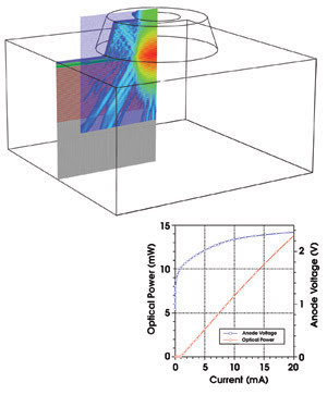
Emphasis must be placed on the solution of the eigenmodes in VCSELs. These devices are becoming key optical communications components because they have several advantages over edge-emitting lasers; e.g., a circular mode shape output, on-chip testing and lower fabrication costs. Dessis calculates the optical mode pattern in a VCSEL using a full-vectorial finite-element algorithm, which allows the accurate calculation of the near and far fields, the cavity resonance and the diffraction loss. Note that approximating the diffraction loss by a less rigorous model introduces uncertainty in predicting the threshold current (Figure 1), in particular, if higher-order modes are analyzed.

Figure 1. In these simulation results for an 850-nm AlGaAs/GaAs VCSEL, the optical mode is solved with the full-wave finite-element solver built into the Dessis device simulator. The result of the eigenmode analysis is the accurate optical field distribution, and a precise prediction of the resonance wavelength and the optical diffraction loss. The electrical device’s behavior and terminal characteristics are calculated in the coupled simulation mode (inset).
VCSEL design
A key objective in VCSEL design is to obtain single-mode lasing up to a high driving current. This can be achieved by proper placement of an oxide aperture, or by patterning the device surface in a way that favors the fundamental mode. In both cases, device engineering introduces a slightly different layer structure, both near- and off-axis. In addition, the oxide aperture strongly influences the current flow. Because the refractive index varies with carrier density and temperature, it is difficult to estimate how the current crowding at the oxide influences the single-mode behavior. And because VCSELs are very small, optical, electronic and thermal effects are strongly coupled.
For the simulation of semiconductor light emitters, an accurate model for the spontaneous and stimulated emission of light is essential. Most of today’s devices have quantum-well active regions, which can be modeled only if relevant physical effects such as carrier capture into — or escape from — the quantum wells are included and are solved consistently.
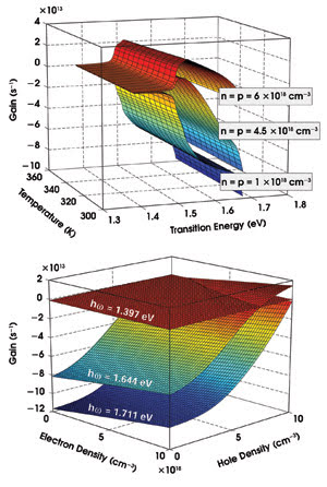
The calculation of the electronic band structure and the optical gain recently garnered significant attention in the modeling community. It has been shown that simplified gain models often fail to predict qualitative and quantitative behavior of modern photonic devices. For a comprehensive simulation, a rigorous calculation based on the so-called k•p method must be applied. The result of the gain calculation can be stored in a gain table, a multidimensional table listing optical material gain as a function of electron and hole densities, temperature and transition energy (Figure 2).

Figure 2. Quantum-well active regions in lasers and LEDs can be characterized by their gain function. Optical material gain is tabulated against electron and hole density, temperature and transition energy. The device simulator can read and write these gain tables.
Although many publications present new and advanced physical models, the amount of time needed for the setup of a device simulation cannot be underestimated. For industrial TCAD, it is important to have state-of-the-art graphical user interfaces for structure generation and visualization of results.
Furthermore, mesh generation is still a critical issue in device simulation because the mesh quality can strongly influence the numerical performance of the simulations.
The numerical models for the design of optoelectronic devices have improved a lot during the past decade, but what makes design a challenge today is that several material parameters are not well-known. An initial effort has to be spent on parameter calibration. By comparing simulation and measurement, a material database that contains a considerable amount of the critical design and manufacturing know-how can be built. Therefore, it is important that the database be completely separate from the simulation model and that its contents be treated as proprietary information.
Although the comprehensive simulation of optoelectronic devices is an involved process, the effort that must be made to numerically solve the coupled optoelectrothermal equations is justified by the insight that engineers can gain from simulation results.
Meet the author
Andreas Witzig is the optoelectronic product manager at ISE Integrated Systems Engineering AG in Zurich, Switzerland; e-mail: [email protected].