Understanding the key differences between CCD and CMOS image sensor technologies will allow distinguishing advantages and limitations of each type of device and help in selecting the optimal device for a given application.
Yakov Bulayev, Hamamatsu Corp.
Since the invention of charge-coupled devices (CCDs) in the 1970s, they have dominated the area of scientific and industrial imaging applications. However, in the 1990s monolithic complementary metal-oxide semiconductor (CMOS) arrays emerged as a serious alternative to CCD image sensors. This was the result of significant improvements in silicon CMOS technology that have been technically and economically driven by digital microelectronics (microprocessors, memory devices, etc.) and applications.
Until recently, CCD image sensors were the sensors of choice for most industrial and scientific applications, while applications of CMOS image sensors were primarily confined to consumer photography. However, recent advances in CMOS sensor technology have rendered these devices an effective imaging solution for numerous industrial, scientific and commercial applications.
CCD image sensors
A CCD image sensor consists of an array of photosensitive charge-coupled elements (pixels). The output signal of the sensor is proportional to the electrical charge accumulated by each pixel in response to irradiation.
Charge transport in a CCD imager is controlled by multiphase — usually two to four — signals that induce potential wells under the electrodes and control the motion of electron packets residing in the potential wells. Charge transport includes transferring charge packets in the columnar direction, as well as clocking off the charge through the horizontal (readout) register to the charge-measurement circuit and output amplifier. This procedure causes charge packets to exit the array of pixels one row at a time.
Among known architectural configurations of CCD imagers, three of the most popular are full-frame, frame transfer and interline. The full-frame architecture, which provides a 100 percent fill factor, is the most universal CCD architecture used for scientific and industrial applications.
Depending on the required spectral response, CCD sensors can be designed for front or back illumination. In front-illuminated devices, light must pass through the polysilicon gate structure located above the photosensitive silicon layer called the “depletion layer.” However, variations in the refraction indices between the polysilicon and silicon structures cause shorter wavelength light to reflect off the CCD surface. This effect, combined with intense UV light absorption in the polysilicon, leads to diminished quantum efficiency (QE) for those wavelengths in the front-illuminated detectors. To improve the overall QE and enable increased CCD sensitivity at UV wavelengths, back-thinned technology can be used. In back-thinned devices, also known as back-illuminated CCDs, the incident photon flux does not have to penetrate the polysilicon gates and is absorbed directly into the silicon pixels.
Concepts of CMOS image sensors
In CMOS arrays, photon-to-voltage conversion occurs inside each pixel1. In general, a CMOS sensor consists of an array of identical pixels; each pixel includes a photodiode and at least one addressing transistor acting as a switch.
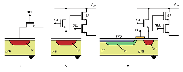 Figure 1. Structure of a passive pixel (a), active pixel (b) and pinned photodiode pixel (c). SEL = addressing transistor. RST = reset transistor. SF = source follower. TX = transfer gate. VDD = power supply voltage. PPD = pinned photodiode.
Originally, CMOS sensors used the so-called passive pixel structure (Figure 1a).
The passive pixel operation:
1. At the beginning of an exposure, the photodiode is reverse-biased on reset.
2. During the exposure time, impinging photons decrease the reverse voltage across the photodiode.
3. At the end of exposure, the remaining voltage across the photodiode is measured; its drop from the original value is used as a measure of the amount of photons falling on the photodiode.
4. The photodiode is reset to be prepared for the next exposure cycle.
The passive pixel sensor (PPS) is characterized by a large fill factor (the ratio of photodiode area to total pixel area), but it suffers from a high noise level. High noise is caused by the mismatch between the small capacitance of the pixel and the large capacitance of the signal bus.
A major improvement in the pixel noise performance was achieved by introducing the active pixel concept, which became very popular in the mid-1990s. In the active pixel sensor (APS), each pixel includes a photodiode, a reset transistor (RST), an addressing transistor (SEL) and a source follower (SF) (Figure 1b).
The principle of operation of the active pixel sensor is similar to that of the passive pixel sensor:
1. The photodiode is reverse-biased on reset.
2. Impinging photons decrease the reverse voltage across the photodiode.
3. At the end of exposure, the pixel is addressed, and the source follower transmits the voltage across the diode outside the pixel.
4. The photodiode is reset once again.
The active pixel structure solved a lot of noise issues. However, the kTC noise caused by resetting the photodiode persisted. To address this issue, a pinned photodiode (PPD) pixel structure was introduced. The PPD pixel (Figure 1c) was a logical improvement to the traditional APS. A pinned photodiode added to the pixel was separated from the readout node by means of a transfer gate (TX). Advantages of the PPD pixel, in comparison with the traditional APS, include low noise performance achieved through correlated double sampling (CDS), and high sensitivity and low dark current of a photodiode.
In a PPD pixel, conversion of the incoming photons is performed in the pinned photodiode. A PPD pixel operates this way:
1. At the end of exposure, the readout node is reset by the reset transistor.
2. The output voltage is measured.
3. The photodiode is drained by activating the TX gate, and the photodiode signal is transferred to the readout node.
4. The output voltage is measured again after the signal has been transferred.
5. CDS signal processing is performed: the second voltage measurement is subtracted from the first measurement.
Since CMOS technology allows integrating the active components into pixels, the pixels can become fully addressable, and on-chip image processing can be performed. To denote the number of transistors in a pixel, the pixels are referred to as 3T, 4T, 5T, etc. Since the PPD pixel usually uses four transistor gates, such an APS pixel is often referred to as a 4T pixel2. As the number of transistors in a pixel increases, functionality and operating flexibility increase, too. When it comes to improved performance, pixels with four or more transistors offer significant noise reductions.
In general, two types of noise — temporal and spatial — should be taken into account when considering an image sensor-based design. One important component of temporal noise that should be considered is the photon shot noise1. The source of this noise is statistical variation in the amount of photons absorbed by the sensor during exposure. This stochastic process can be described by Poisson statistics. Let’s assume that during the exposure a pixel receives an average amount of photons equal to µph. This average value is characterized by a noise component σph, representing the photon shot noise. The relationship between the average value µph and its associated noise can be described as:
After the absorption of incoming photons by a pixel, the flux of µph photons results in µe electrons stored in this pixel. These electrons are characterized by a noise component σe, that also has a square root relationship with µe. Assuming that we are dealing with a hypothetical noise-free imager and noise-free electronics, the performance of the image sensor-based system will be limited by photon shot noise. The maximum signal-to-noise ratio is described by the following equation:
Since the maximum signal-to-noise ratio equals the square root of the signal value, the minimum pixel dimensions will be limited not by the CMOS technology but by the number of electrons that can be stored in the pixel1.
There are two types of CMOS image sensors currently available on the market: CMOS linear image sensors and CMOS area (2D) image sensors.
CMOS linear image sensors
Improved features and characteristics of CMOS linear image sensors make them suitable for various applications including spectroscopy, machine vision and barcode scanning.
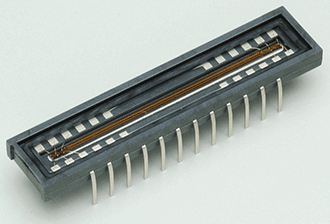
Figure 2. CMOS linear image sensor S11639.
For example, manufacturers of spectroscopy instruments welcomed the Hamamatsu S11639 CMOS linear image sensor (Figure 2) as an alternative to CCD sensors.
The pixel format of this active pixel sensor is optimized for spectroscopy applications. Also, most of its performance characteristics are comparable with those of the time-honored Sony ILX511 CCD sensor or exceed them. This Hamamatsu sensor has a spectral response range from UV to NIR (Figure 3) without the need for any additional coating and meets the requirements of spectroscopy systems for image sensors.
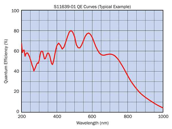 Figure 3. Spectral response of the S11639 sensor.
In addition to spectroscopy applications, the S11639 sensor can also be used for position detection, image reading, encoding and other machine vision applications.
One of the advantages of CMOS technology is that it allows integration into a CMOS sensor of different circuitries that can perform signal processing, timing generation, analog-to-digital conversion, electronic shutter, variable integration time, interfacing and other functions.
For example, a sensor that features a variable integration time function is beneficial for some spectrophotometry instruments. This function is performed by means of an embedded shift register (Figure 4) that allows resetting specific pixels during the readout cycle or letting the pixels absorb incoming photons without being reset, until the next readout cycle. The ON or OFF condition of the address switches S1-Sn of each pixel is controlled by the integration time control signal (INT) that is synchronized with the clock signal (CLK).
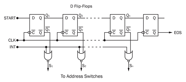 Figure 4. Shift register for readout control. CLK = clock signal. INT = integration time control signal. D, Q, C = attributes of standard D Flip-flop. S1 - Sn = address switches of the pixels. EOS = end of scan signal.
Another feature of CMOS image sensors where significant improvements can be observed is packaging. COB (chip-on-board) technology has allowed the building of CMOS linear image sensors (Figure 5) measuring only 0.8 mm in thickness. These sensors are half the thickness of previously available devices.
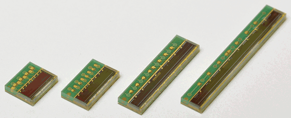
Figure 5. COB packaged CMOS linear image sensors.
These thin COB sensors can be used for barcode readers, encoders and various types of image scanning applications including handheld scanners and other devices that need to integrate compact and cost-effective sensors.
CMOS area image sensors
Advances in CMOS technology have also brought to the market CMOS area image sensors that can be used for industrial and security applications (Figure 6). These are offered in several formats including: SXGA (1280 × 1024 pixels), VGA (640 × 480 pixels), and QVGA (320 × 240 pixels).
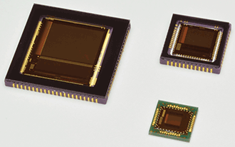
Figure 6. CMOS area image sensors with SXGA, VGA and QVGA pixel format.
These sensors can be used for various industrial applications including machine vision, coin detection, fingerprint pattern imaging, as well as for vein pattern imaging and other medical imaging applications. Since these sensors are sensitive in the near infrared (NIR) region, they also can be used for different NIR security applications, as well as for position and shape recognition applications.
Over the last decade, CMOS image sensor technology has experienced great progress. Not only have CMOS image sensors been able to penetrate and gain ground in markets previously dominated by CCD sensors, but they have also found new and original applications.
References
1. A. Theuwissen (May 2008). CMOS image sensors: State-of-the-art. Solid-State Electron, Vol. 52, No. 9, pp. 1401-1406.
2. E. Fossum and D. Hondongwa (February 2014). A review of pinned photodiode CCD and CMOS image sensors. IEEE J Electron Devices Soc, Vol. 2, No. 3, pp. 33-43.
Acknowledgments
The author would like to thank Masaharu Muramatsu and Yoshihito Ito (Hamamatsu Photonics K.K.) for reviewing this article and giving their helpful suggestions. He also wants to thank Maridel Lares (Hamamatsu Corp.) for her great support in preparation of this article.
About the author
Yakov Bulayev is a product manager at Hamamatsu Corp. He is a member of SPIE and IEEE professional societies; email: [email protected].