
Additive Manufacturing Solution Provider NEMATX Earns Investment: Week in Brief 08/02/24
LONDON, Aug. 2, 2024 — The U.K. is funding five quantum hubs with £100 million ($128 million) to support the development of practical applications for quantum technologies in areas like medical scanning, secure communications, and next generation positioning systems. The hubs are to be led by leading universities who will work closely with industrial partners. The UK Quantum Biomedical Sensing Research Hub is to be led by University College London and the University of Cambridge; the UK Quantum Technology Hub in Sensing, Imaging and Timing will be headed by the University of Birmingham; the Integrated Quantum Networks Quantum Technology Hub by Heriot-Watt University, the Hub for Quantum Computing via Integrated and Interconnected Implementations by the University of Oxford, and the UK Hub for Quantum Enabled Position, Navigation and Timing will be led by the University of Glasgow.
SEATTLE — NLM Photonics was awarded a $1.8 million contract from the U.S. Air Force to fund a 21-month project with AIM Photonics. The project aims to offer modulator components in AIM Photonics’ process design kits for silicon-organic hybrid devices on the institute’s 300-mm silicon photonics platform. These devices focus on low-power, high-bandwidth electro-optic (EO) modulation for datacom, radio frequency photonics, sensing, and other applications using silicon-organic hybrid EO modulators. NLM will perform process development and optimization, and work with the AIM Photonics’ Test, Assembly, and Packaging facility for wafer-scale passive and die-level high-speed device testing.
ITZEHOE, Germany — Augmented reality technology company OQmented partnered with laser chip developer Brilliance to advance laser beam scanning technology applications. The collaboration aims to integrate Brilliance’s laser chips with OQmented light engines, both of which are assembled at the wafer level. The strategy for their combination is expected to provide significant cost savings compared to conventional processes.
CENTENNIAL, Colo. — NUBURU, a developer of high-power and high-brightness industrial blue laser technology, received notice from NYSE American LLC informing NUBURU that it has withdrawn its delisting determination and will be lifting the trading suspension on NUBURU common stock on NYSE American. In January, NUBURU received a deficiency letter because of noncompliance with continued listing standards.
TORONTO — POET Technologies, a developer of optical technologies for data center, telecommunication, and AI markets, expanded its partnership with Luxshare Technology to provide more optical module products targeted at AI network equipment and AI service providers. The companies will produce additional types of optical transceiver modules that will include POET’s transmit and receive optical engines for Luxshare’s 400G and 800G pluggable transceivers for single mode fiber applications. The optical modules will be manufactured and sold globally by Luxshare Technology.
BOSTON — Dotmatics, a provider of R&D software, acquired EasyPanel, a specialist in flow cytometry panel design software. Flow cytometry panel design refers to the process of selecting and combining specific fluorophores and antibodies to analyze multiple parameters simultaneously on individual cells within a biological sample. According to Dotmatics, it is the initial step in the flow cytometry phenotyping process, occurring before panel preparation in the wet lab, data acquisition on a flow cytometer, and subsequent analysis using software like Dotmatics’ FCS Express and OMIQ.
SANTA CLARA, Calif. — Agilent Technologies, a provider of analytical and laboratory technologies including instruments for molecular spectroscopy, acquired Sigsense Technologies, a startup using AI and power monitoring to help optimize lab operations. Sigsense technology is already integrated into the Agilent CrossLab Connect asset monitoring solution. Sigsense’s algorithm tracks instrument use and status across all scientific assets, regardless of vendor or manufacturer. The operational insights collected from the technology alert lab managers of assets that are underperforming and how to optimize them. Financial terms of the acquisition were not disclosed.
FARNBOROUGH, England — Aerospace ecosystem solutions provider GA Telesis partnered with Alitheon, a developer of optical AI for no-touch serialization, to integrate Alitheon’s "FeaturePrint" technology into GA Telesis’ WILBUR platform. FeaturePrint’s algorithms leverage standard industrial cameras or mobile phones to create a unique digital fingerprint based on the minute surface details of physical objects. The collaboration aims to increase safety in the aviation and aerospace supply chain.
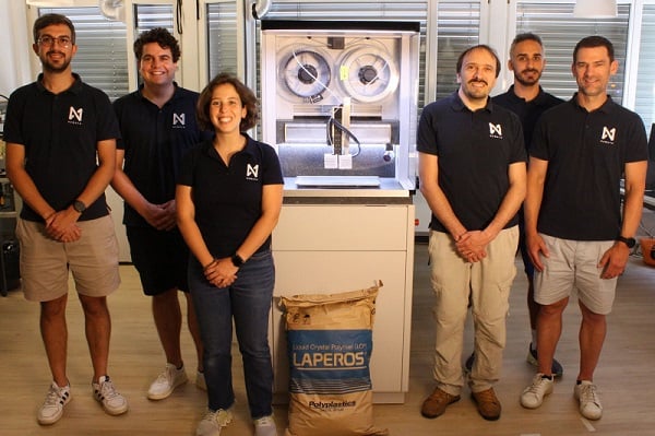
Through its partnership with POLYPLASTICS, 3D printing company NEMATX will advance its capabilities in additive manufacturing to produce high resolution, thermally stable components with desirable mechanical and chemical properties. Courtesy of NEMATX.
ZÜRICH — Industrial 3D printing and materials company and ETH Zurich spin-off NEMATX AG received a strategic investment from POLYPLASTICS Co., Ltd., a leader in the development and production of high-performance plastics. Through the partnership, NEMATX, a developer of a liquid crystal polymer/additive manufacturing solution, will be able to leverage POLYPLASTICS’ expertise in plastics processing into its own product development. This will enable the company to offer customized additive manufacturing solutions for components that have a previously unattainable combination of 3D printing resolution, thermal stability, and mechanical and chemical properties.
MUNICH — Inova Semiconductors and Lextar, a subsidiary of Ennostar, signed a memorandum of understanding under which Inova will provide its intelligent smart embedded LED (ISELED) and ISSELED light and sensor network technology to Lextar, a Taiwan-based LED optoelectronics technology solutions provider. Lextar intends to build smart LED products to enhance its ISELED product portfolio for automotive applications such as functional and decorative interior and exterior lighting.
/Buyers_Guide/NLM_Photonics/c33430
/Buyers_Guide/AIM_Photonics/c33819
/Buyers_Guide/OQmented_GmbH/c32312
/Buyers_Guide/Brilliance_BV/c33640
/Buyers_Guide/Nuburu_Inc/c31283
/Buyers_Guide/POET_Technologies/c31036
/Buyers_Guide/Luxshare_Technology_Co_Ltd/c33455
/Buyers_Guide/Agilent_Technologies_Inc/c25255
/Buyers_Guide/Dotmatics/c21003
/Buyers_Guide/Inova_Semiconductors_GmbH/c6790
/Buyers_Guide/Lextar_Electronics_Corp/c24884