Recent advances in vertical-cavity surface-emitting lasers yield novel high-power, high-reliability lasers for industry, medicine and defense.
Jean-François Seurin, L. Arthur D’Asaro and Chuni Ghosh, Princeton Optronics Inc.
Compact and robust high-power semiconductor lasers are needed in a variety of applications; foremost is pumping of solid-state and fiber lasers. Presently, semiconductor edge-emitters dominate the market for pump lasers. However, edge-emitters have several drawbacks, such as poor intrinsic beam profile and spectral properties as well as generally low array reliability. In addition, scaling up the output power requires the complex and costly assembly of edge-emitting bars into stacks.
Vertical-cavity surface-emitting lasers (VCSELs) present an attractive alternative as a high-power semiconductor laser source (several hundred watts) because they easily can be processed into 2-D arrays to scale up the power.1 However, to the best of our knowledge, no current commercial system uses VCSELs as pump sources.
We recently used a relatively small VCSEL 2-D array (~0.22 cm2 array area) to demonstrate more than 230 W of CW output power, corresponding to more than 1 kW/cm2 power density (Figure 1). We also have demonstrated 100 W from quasi-CW small arrays (~0.028 cm2 array area), corresponding to more than 3.5 kW/cm2 power density. These CW and quasi-CW power density levels are comparable to those of edge-emitters.
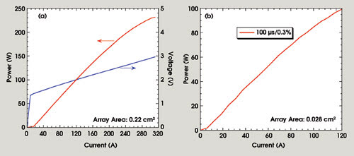
Figure 1. The plot in (a) shows output power (red) and voltage (blue) taken at room temperature for a high-power 2-D VCSEL array. The maximum power is 231 W. In (b), the plot shows the quasi-CW output power versus injection current at room temperature for a 100-μs pulse width and 0.3 percent duty cycle. This array reaches a maximum power of 100 W and a maximum power density of 3.5 kW/cm2.
Ironically, VCSELs’ rise to fame originated in low-power (submilliwatt) applications. They were invented in the mid-1980s and quickly gained a reputation as a superior technology for short-reach telecom applications such as fiber-channel, Ethernet and intrasystems links. Within the first two years of their commercial availability (~1996), they became the technology of choice for local area networks, effectively displacing edge-emitters. This success was the result primarily of the lower manufacturing costs and higher reliability of VCSELs compared with edge-emitters.2
Simple planar processing
To comprehend how a VCSEL works and what its key advantages are over edge-emitters, it is important to understand the fabrication processes for both technologies (Figure 2).
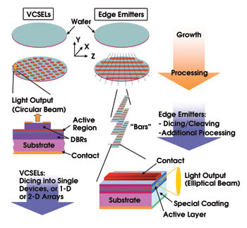
Figure 2. The fabrication process for VCSELs and edge-emitter semiconductor lasers is shown from top to bottom. Epitaxial material is first grown on GaAs substrates (typically 3 or 4 in. in diameter). The wafers are processed into single devices using standard photolithography, metallization and surface passivation, as well as wet and/or dry etching. In addition, for VCSELs, selective oxidation or ion implantation is used for current confinement. At this point, VCSEL devices are completed and can be tested at the wafer level (the light emits perpendicular to the wafer). Edge-emitters, on the other hand, must be diced into bars and undergo a delicate facet coating before being tested. After wafer-level selection of good devices, VCSELs can be cleaved into single devices, or into 1- or 2-D arrays.
Semiconductor lasers consist of layers of semiconductor material grown on top of each other on a substrate (the “epitaxial” structure). For VCSELs and edge-emitters, this growth is done typically in a molecular-beam-epitaxy or metal-organic-chemical-vapor-deposition growth reactor. The grown wafer is processed accordingly to produce individual devices.
In a VCSEL, the active layer is sandwiched between two highly reflective mirrors (actually distributed Bragg reflectors) made up of several quarter-wavelength-thick layers of semiconductors of alternating high and low refractive index. The reflectivity of these mirrors is typically in the range of 99.5 to ~99.9 percent. As a result, the light oscillates perpendicular to the layers and escapes through the top (or bottom) of the device.
Current and/or optical confinement is achieved typically through either selective oxidation of an aluminum-rich layer, or through ion implantation (or even both for certain applications) (Figure 3). VCSELs can be designed for top emission at the epitaxial/air interface or bottom emission through the transparent substrate, in cases where junction-down soldering is required for more efficient heat sinking, for example.
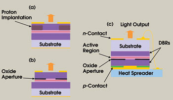
Figure 3. Three common types of VCSEL structures are a top-emitting structure with proton implantation to confine the current (a), a selectively oxidized top-emitting structure to confine the optical modes and/or the current (b), and a mounted bottom-emitting selectively oxidized structure (c).
Because VCSELs are grown, processed and tested while still in the wafer form, there is significant economy of scale resulting from the ability to conduct parallel device processing, whereby equipment utilization and yields are maximized and setup times and labor content are minimized. In fact, VCSEL processing is identical to the well-established, low-cost silicon integrated-circuit planar processing.
In the case of a VCSEL, the mirrors and active region are sequentially stacked along the Y- (i.e., vertical) axis during epitaxial growth. The wafer goes through etching and metallization steps to form the electrical contacts. At this point, the wafer goes to test where individual laser devices are characterized on a pass-fail basis. Finally, the wafer is diced, and the good lasers (yield typically is greater than 95 percent) move on to higher-level assembly. The wafer can be diced into single devices or into arrays of single devices effectively connected in parallel. The arrays can be linear (1-D), rectangular or square (2-D).
Furthermore, because the positions of the individual elements in a VCSEL array are defined by photo-lithography, arbitrary design layouts of the elements with placement accuracy at the micron level are possible. Depending on the application, VCSEL 2-D arrays can contain between a few hundred and several thousand single devices. Figure 4 shows a fully packaged high-power VCSEL array assembled on a microcooler.
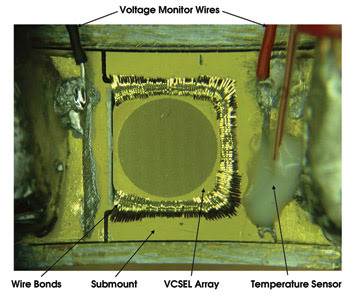
Figure 4. This high-power, 2-D VCSEL array is mounted on a microcooler for efficient heat removal at high powers. The array chip is approximately 5 × 5 mm.
Edge-emitter fabrication
For edge-emitters, the growth process also occurs along the Y-axis, but only to create the active region, because mirror coatings are applied later along the Z- (i.e., horizontal) axis. After epitaxial growth, the wafer undergoes the metallization step and is subsequently cleaved along the X-axis, forming a series of wafer strips which are stacked and mounted into a coating fixture. The Z-axis edges of the wafer strips are coated to form the device mirrors.
On the emission facet, the coating is typically designed for less than 5 percent reflectivity. This coating is a critical processing step for edge-emitters because any coating imperfection will result in early and catastrophic failure of the devices from so-called catastrophic optical damage. This failure mode has been a major reliability and yield issue for edge-emitters.
After this coating step, the wafer strips are diced to form discrete laser chips or “bars” (linear arrays), which are mounted onto carriers. Finally, the laser devices are tested. Clearly, edge-emitters cannot be processed into 2-D monolithic arrays. Scaling of the power requires time-consuming and expensive assembly of bars into stacks.
Very high reliability
In terms of reliability, VCSELs have an inherent advantage over edge-emitters because they are not subject to catastrophic optical damage. In the case of edge-emitters, the emission surface is small, leading to high power densities at the output facet, where the p-n junction intersects the emission surface. If care is not taken to properly passivate this surface (by using some dielectric coating, for example), the semiconductor gain material will rapidly degrade in that region because of high localized increase in temperature, leading to catastrophic optical damage. This failure mechanism is sensitive to the quality of the coating as well as to junction temperature. VCSELs, on the other hand, are not sensitive to surface conditions because the gain region is embedded in the epitaxial structure and does not interact with the emission surface and because the power densities involved are much smaller.
Over the years, several reliability studies for VCSELs have yielded failures-in-time rates (that is, the number of failures in one billion device-hours) on the order of 10 or less,3 whereas for the highest telecom-grade edge-emitters these rates are on the order of 500.4 The failure rate for industry-grade high-power edge-emitter bars or stacks is generally worse. This reliability advantage is important for laser systems where the end-of-life and field failures are dominated overwhelmingly by pump-laser failure.
Activation energy (EA) is generally used to describe the temperature dependence of the failures associated with a particular technology. This parameter is derived through a plot of the mean time to failure as a function of the inverse junction temperature. In the case of edge-emitters, because catastrophic optical damage is sensitive to the facet temperature, their activation energy is typically on the order of 0.45 eV. But because VCSELs are not subject to catastrophic optical damage, the activation energy is almost twice as high as that of edge-emitters (~0.7 eV). This means that VCSELs can be reliably operated at higher temperatures.5 This advantage is significant because the requirements for refrigeration become less strict for VCSELs, resulting in a more compact laser system with higher overall efficiency.
Spectral and beam quality
Unique spectral and beam properties greatly helped low-power VCSELs conquer the short-reach telecom markets. As it turns out, these properties are equally advantageous for high-power applications.
Because the VCSEL resonant cavity is defined by a wavelength-thick cavity sandwiched between two distributed Bragg reflectors, devices emit in a single longitudinal mode, and the emission wavelength is inherently stable (~0.065 nm/K, compared with ~0.3 nm/K for edge-emitters), without the need for additional wavelength stabilization schemes or external optics, as is necessary for edge-emitters. Furthermore, thanks to advances in growth and packaging technologies, the emission wavelength is uniform across large VCSEL 2-D arrays, resulting in spectral widths of ~0.8 nm (Figure 5a), which is significantly lower than for edge-emitters (3 to ~5 nm). This wavelength stability and narrow spectral width are useful in many pumping applications where the medium has a narrow absorption band.
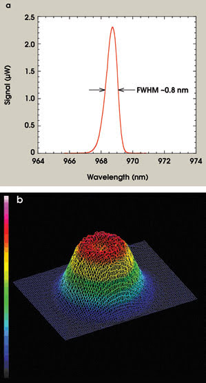
Figure 5. The spectrum of a 100-W, CW 2-D VCSEL array has a full width half maximum of 0.8 nm (a). The corresponding output beam is circular with a full-width divergence angle of 17° and a flat-top, far-field profile (b).
Unlike edge-emitters, VCSELs emit a circularly symmetric beam with low divergence, without the requirement of additional optics. This low divergence has been a tremendous advantage for low-power VCSELs in the telecom and datacom markets because of their ability to directly couple to fibers (butt-coupling) with high efficiency.
As can be seen from Figure 5b, high-power VCSEL arrays emit in a circular, low-divergence, quasi-top-hat beam profile, making these devices ideal for end-pumping of solid-state lasers.
In addition, the reflectivity of the as-grown distributed Bragg reflector that serves as the output coupler is high in VCSELs (typically greater than 99.5 percent) as compared with edge-emitters (typically less than 5 percent). This design makes VCSELs extremely insensitive to optical feedback effects, thus eliminating the need for expensive isolators or filters in many applications.
Outlook
VCSELs, because of their significant and unique advantages in terms of cost, reliability and performance could become the next technology of choice for compact and efficient high-power semiconductor laser sources.
Some challenges remain before VCSELs can start taking significant shares of the high-power markets, however. First, although the reliability of single-VCSEL devices is well established, long-term aging data is lacking for large, high-power arrays because this is a relatively young technology. Second, although the wall-plug efficiency has improved significantly in recent years, it still lags a bit behind that of edge-emitters (~55 percent for commercial products). Still, because VCSELs can operate reliably at high temperatures, the overall system efficiency could be higher because no refrigeration apparatus would be needed.
Finally, in terms of brightness (defined as the power divided by the square of the beam-size divergence product), edge-emitters are ahead of VCSELs, even though complex optics are required for edge-emitter bars or stacks to achieve high brightness. This is mainly because single edge-emitter devices can achieve high power densities (a few watts from an ~2 × 100-μm emission area) compared with VCSELs.
In the near future, we plan to increase the CW power density to 2 kW/cm2 and the quasi-CW power density to 6 kW/cm2. We also plan to develop high-brightness, high-power VCSEL sources for specific applications such as pumping of fiber lasers.
Acknowledgments
We are grateful for the support from the DARPA Super High Efficiency Diode Sources program (SHEDS).
Meet the authors
Jean-François Seurin is director of device research and development at Princeton Optronics; e-mail: [email protected].
L. Arthur D’Asaro is a senior member of the technical staff at Princeton Optronics, Mercerville, N.J.; e-mail: [email protected].
Chuni Ghosh is president and founder of Princeton Optronics; e-mail: [email protected].
References
1. L.A. D’Asaro et al (February 2005). High-power, high-efficiency VCSELs pursue the goal. Photonics Spectra, pp. 62-66.
2. K.S. Giboney et al (February 1998). The ideal light source for datanets. IEEE Spectrum, Vol. 35, pp. 43-53.
3. J.A. Tatum et al (May 2000). Commercialization of Honeywell’s VCSEL technology. Proceedings of the SPIE, Vol. 3946, pp. 2-13.
4. H.-U. Pfeiffer et al (March 2002). Reliability of 980-nm pump lasers for submarine, long-haul terrestrial, and low cost metro applications. Optical Fiber Communication Conference (OFC), 2002, pp.
5. A. Morgan et al (May 1995). 200 °C, 96-nm wavelength range, continuous-wave lasing from unbonded GaAs MOVPE-grown vertical cavity surface-emitting lasers. IEEE Photonics Technology Letters, Vol. 7, pp. 441-443.