The first electrically pumped, hybrid silicon laser overcomes one of the last major hurdles to silicon photonic chips.
Richard Jones, Oded Cohen and Mario Paniccia, Intel Corp., and Alexander W. Fang, Hyundai Park and John Bowers, University of California, Santa Barbara
Silicon photonics holds the potential to create low-cost, highly integrated optical components using the same CMOS-based manufacturing techniques that have revolutionized the electronics industry over the past 40 years. This potential is important, as it could enable high-bandwidth optical communication links in and around personal computers and servers that, to date, have been prohibitively expensive.
Silicon has many unique properties that are optimal for optical communications. For example, its transparency at wavelengths above 1.1 μm makes it compatible with long-wavelength infrared communication links. In addition, its high-index contrast with silicon dioxide (Δn~2) enables integrated optical devices with small footprints.
Research is being conducted worldwide to prove silicon’s suitability as an optical material and to demonstrate the basic components needed for a silicon-based optical link. For example, Raman amplification has been used to demonstrate optically pumped lasing in silicon using on-chip, ring-resonator-based cavities.1 Other research has demonstrated a high-speed optical modulator with bandwidths greater than 10 Gb/s, a speed that is useful for today’s optical networks.2 And germanium, or silicon germanium (SiGe), has been used to manufacture high-speed photodetectors that are sensitive in the infrared, where silicon’s transparency means that it cannot be used to detect light.3
These research breakthroughs clearly prove that silicon may be considered a useful material for building optical components. However, the lack of an electrically pumped laser — the Raman laser is optically pumped — that can be easily integrated with other silicon devices has been key to stifling the commercialization of silicon photonics.
Currently, individual prefabricated lasers may be integrated with silicon by aligning and attaching them to the silicon photonic die one at a time. A significant drawback to this method is that the assembly time increases as the number of lasers increases. Consider, for example, a silicon wafer containing hundreds of devices, all processed simultaneously using planar CMOS manufacturing. Individually attaching a laser to each of a few hundred devices per wafer is clearly not a time- or cost-efficient solution. A better approach would be to use the same wafer-scale fabrication techniques to manufacture both the silicon components and the laser. That is the aim of the work discussed here.
Various methods have been proposed to integrate a laser with silicon photonics. Although the most straightforward is the true silicon laser, there is a fundamental physics barrier prohibiting this alternative. We have pursued a heterogeneous option, which is the integration of multiple material systems onto a common substrate. This technique combines the light-emitting properties of indium phosphide with the light-routing capabilities of silicon in a single hybrid chip. Using a unique bonding technique, we recently demonstrated the first electrically pumped hybrid-silicon laser.4
Silicon laser
Clearly, a laser fabricated from pure silicon would be ideal for a light source because it could be monolithically fabricated on the same chip as the other silicon photonic components. Alignment would be built into the fabrication process, eliminating the need to assemble and align separate components, and one could envision an entire optical integrated circuit — containing multiple lasers and other components —fabricated for a fraction of the cost of assembling and aligning separate discrete devices.
Unfortunately, silicon’s indirect bandgap makes light emission in the bulk material highly inefficient. Thus, it is extremely difficult to fabricate any kind of light emitter with this material. Scientists worldwide have been trying to finesse this problem, investigating, for example, the light-emission properties of porous and doped nanostructured silicon. However, to date, an electrically pumped pure silicon laser has not been demonstrated.
The only demonstration of lasing in silicon thus far has been achieved using Raman amplification. Unfortunately, this solution does not alleviate the laser packaging problem because Raman amplification requires optical pumping, which means that another laser is needed as a power source. Therefore, this approach is not the most likely candidate for a low-cost silicon laser for use in optical interconnects in and around PCs and servers. However, the recent demonstration of silicon Raman amplifiers and wavelength converters at data rates as high as 40 Gb/s point to many other uses of silicon nonlinear devices for optical communications.
Until an electrically pumped silicon laser is demonstrated, III-V semiconductor materials will continue to be necessary to produce communication lasers. One must then determine how these optical sources can be integrated cost-effectively onto a silicon photonic chip. Figure 1 shows a simple schematic of various methods for bringing a III-V-based light source onto a silicon photonic chip.
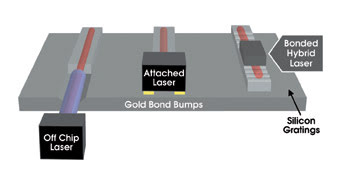
Figure 1. Three methods for integrating a laser into a silicon device are represented by (left to right) an off-chip laser, an on-chip laser and a hybrid laser.
Off-chip or on-chip
Perhaps the most straightforward way to introduce light into a silicon photonic device is with a fiber-coupled laser. The fiber delivering the laser’s energy could be connected and passively aligned to the silicon die. Once into the silicon, the laser light could be split into separate channels, each of which could be modulated before being recombined and transmitted. This is directly analogous to the way an electrical supply powers an integrated circuit today. One advantage of this method is its flexibility with regard to choosing the laser source, because many fiber-coupled sources are already commercially available. Another advantage is that the laser is separate from the silicon device, allowing better thermal management of the photonics system. The disadvantages of this approach are the relatively high cost for the laser sources, the laser size and the nonintegrated packaging complexity.
A better solution for coupling light into a silicon photonic chip is to bond, or solder, individual low-cost lasers directly to the silicon chip using mechanical stops and metal patterning to align the lasers. The problem here is that submicron alignment accuracy is needed when coupling to small single-mode waveguides, which is hard to achieve in a manufacturing environment with the standard high-volume pick-and-place tools available. Moreover, because each laser must be placed and aligned individually, the assembly time increases linearly with the number of lasers required. As the number of lasers per chip increases, this alternative becomes prohibitively inefficient and costly.
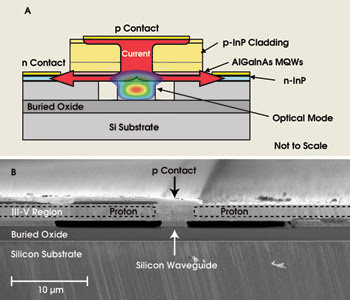
Figure 2. This schematic of a hybrid silicon laser (A) identifies the key components found in the scanning electron micrograph of the fabricated device (B).
Hybrid approach
A third approach using the hybrid silicon laser was developed recently in a collaboration between the University of California, Santa Barbara, and Intel Corp. (Figure 2). The technique overcomes the many problems inherent in the previous integration strategies by employing a volume-manufacturable wafer-bonding process wherein an unprocessed III-V wafer is bonded to a silicon wafer patterned with optical waveguides. Multiple hybrid lasers are then fabricated simultaneously across the wafer using standard planar-fabrication techniques. Because the silicon waveguides are patterned before laser fabrication, no alignment is needed between the unpatterned III-V wafer and the patterned silicon wafer. Using this method, we believe that tens — if not hundreds — of lasers can be fabricated simultaneously across a die with a single bonding step. Fabrication may take place at the wafer, partial-wafer or die-level, depending on the exact application and economics of the device being fabricated.
The laser mode is guided in the silicon waveguide, while electrical pumping and light emission take place in the AlGaInAs quantum wells in the III-V material. The gain is proportional to the overlap between the hybrid-waveguide mode and the quantum-well region and can be varied by adjusting both the height and the width of the silicon waveguide.
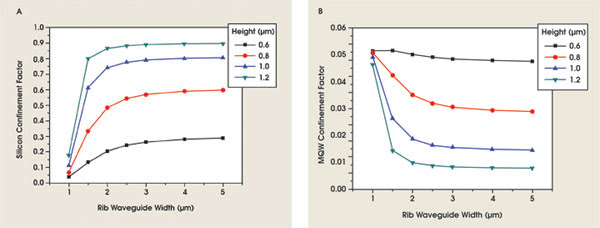
Figure 3. These plots show the calculated confinement factor in the silicon (A) and quantum-well region (B) as a function of waveguide height and width (MQW = multiple quantum wells).
Figure 3 shows how the mode overlap of the active quantum well layer and the silicon waveguide varies with the silicon waveguide dimensions. The figure clearly shows that decreasing the silicon waveguide width and/or height pushes the optical mode into the III-V quantum-well region, increasing the gain. Widening the silicon waveguide increases the mode overlap with the silicon waveguide, which is important for efficient coupling of the laser output light into other silicon photonic devices. In the current proof-of-concept design, the mode overlap with the offset quantum well region is about 3 percent. This is slightly less than that for conventional III-V lasers (typically 5 to 10 percent), but it provides sufficient gain to allow lasing in this hybrid silicon laser architecture.
Wafer bonding and fabrication
Fabrication of the hybrid silicon laser is performed using a low-temperature (~300 °C) wafer-bonding technique. Bonding the two material systems addresses the difficulties of lattice mismatch that occur when attempts are made to grow III-V materials directly onto silicon. The low-temperature bonding allows for the different thermal expansion coefficients of the two materials and eliminates any pronounced stress in the final bonded system.
The key to this wafer-bonding technique is the thin oxide “glue” that bonds the two materials together. Before bonding, the silicon photonic chip and the III-V wafers are exposed to an oxygen plasma wherein an ~50-atom-thick layer of oxide is grown onto each surface. The two wafers are then bonded at a temperature of 300 °C with an applied pressure of 1.5 MPa for ~12 hours.
The bonded device then has some simple back-end fabrication processing, including a proton implantation to help confine the current injection to the center of the waveguide, and depositing and patterning of the metal electrical contacts (Figure 2). The hybrid lasers are diced and both facets polished to form bars of 36 Fabry-Perot lasers, each about 800 μm long. More details on the hybrid silicon laser fabrication and multiple quantum wells structures can be found in referenced literature.1
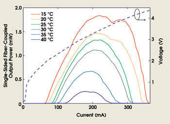
Figure 4. This figure shows the laser output power coupled from one facet of the hybrid laser into a single-mode lensed fiber as a function of the applied bias current, for operating temperatures from 15 to 40 °C. The hybrid silicon laser generated up to 1.8 mW when operated at 15 °C.
Results
The laser has a maximum output power of 1.8 mW at 15 °C, with a threshold of ~65 mA at 2V (Figure 4). The differential quantum efficiency — defined as the number of photons emitted per electron injected above laser threshold — is calculated to be ~12.7 percent (taking into account the 6-dB coupling loss from the silicon waveguide to the lensed fiber and the fact that light is collected from only one facet). The output light is horizontally (TE) polarized, which is dictated by the orientation of the offset III-V quantum well region in the plane of the III-V wafer. The laser has a 40 °C maximum lasing temperature with a characteristic temperature of 39 K.
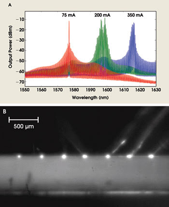
Figure 5. The output shifts to longer wavelengths as the laser’s temperature increases (A). An infrared-camera image shows the output from seven biased lasers in the same monolithic bar (B). Mechanical constraints in the laboratory prevented biasing more than seven lasers.
A collection of output spectra from these first-generation devices is shown in Figure 5a. As is typical for Fabry-Perot lasers, these hybrid lasers support multiple longitudinal modes. In addition, as shown in the figure, the lasing wavelength shifts to longer wavelengths as the bias current is increased. This shift is typical for semiconductor lasers and is the result of ohmic heating and temperature-induced bandgap shrinkage of the active region.
Figure 5B is the imaged output facet (using an infrared camera) of seven continuous-wave hybrid silicon lasers operating simultaneously from a single bonded-silicon chip, which shows the scalable nature of the technique. The white dots across the center of the chip are the lasers emitting from the hybrid-laser facets (see center section of Figure 5B), and the angled electrical probes that power the lasers are seen directly above them. The limit of seven hybrid lasers operating simultaneously was a constraint of the electrical probes setup and not of the number of functional hybrid lasers. In this specific sample, 30 of the 36 lasers on this bonded chip were operational, all with equivalent performance characteristics as discussed above.
Future work
The results described herein were obtained with our first-generation hybrid silicon laser devices. Future work will focus on demonstrating single-wavelength laser performance, lowering the laser threshold to ~20 mA and improving the laser maximum operating temperature.
Devices employed thus far were simple Fabry-Perot lasers relying on the Fresnel reflection (~30 percent) from the hybrid waveguide-air interface to create the laser cavity. Single-wavelength lasers may be fabricated by designing on-chip laser cavities with wavelength-selective elements such as gratings or by using small and compact ring resonators patterned into the silicon photonic chip. Because the laser characteristics are determined by the silicon waveguide, one can imagine obtaining very narrow, single-wavelength performance using the advanced lithography tools found in today’s leading-edge CMOS fabrication facilities.
Reducing laser threshold and improving laser operating temperature can be accomplished by reducing ohmic resistance and improving overall thermal conductivity. In these first-generation devices, the separation from the negative contact to the center of the waveguide was about 38 μm (Figure 2B). Simulations show that reducing this contact separation to less than 10 μm and thinning the buried oxide of the silicon wafer from 2 to 1 μm should significantly improve the performance of the laser as it reduces ohmic heating and enhances overall heat dissipation.
Derivatives of this architecture also could be used to fabricate other hybrid devices on silicon, and work is being done to investigate instruments such as power monitors, photodetectors, optical amplifiers and modulators. Various III-V active regions also may be bonded onto areas of the silicon chip using a technique called nonplanar wafer bonding. This could allow both 1310- and 1550-nm devices to be fabricated on a single die, which is important for applications such as fiber-to-the-home.
The demonstration of an electrically pumped hybrid silicon laser addresses one of the last major barriers to producing low-cost, high-bandwidth silicon photonic devices for use in and around computers and data centers. Currently, the microprocessor industry is moving from single-core microprocessors to dual- and quad-core processors, with future ones potentially having more than 100 cores on a single chip. These hundreds of processing cores will need to be fed terabits of information, and low-cost, highly integrated optical links will be essential to achieving this.
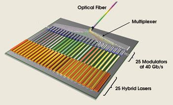
Figure 6. The hybrid-silicon technology could allow a terabit silicon optical transmitter chip consisting of a row of 25 single-wavelength hybrid-silicon lasers, such as the one seen here.
Figure 6 is a schematic of a proposed terabit silicon optical transmitter chip consisting of a row of 25 single-wavelength hybrid-silicon lasers, each integrated with its own 40-Gb/s silicon modulator. The 25 wavelengths are combined into a single output waveguide with a silicon multiplexer. It is envisioned that this integrated chip, which would be too costly to build if each laser had to be aligned individually, could be used to connect optical backplanes or to make connections between future servers and PCs.
In addition, this hybrid silicon laser architecture could be used for other applications that require low-cost integrated optical devices ranging from fiber-to-the-home to biosensing and lab-on-a-chip applications.
References
1. H. Rong et al (2006). Monolithic integrated Raman silicon laser. OPT EXPRESS, Vol. 14, pp. 6705-6712.
2. L. Liao et al (2005). High Speed Silicon Mach-Zehnder Modulator. OPT EXPRESS, Vol. 13, pp. 3129-3135.
3. J. Liu et al (2005). Tensile strained Ge p-i-n photodetectors on Si platform for C and L band telecommunications. APPL PHYS LETT, Vol. 87, 011110.
4. A.W. Fang et al (2006). Electrically pumped hybrid AlGaInAs-silicon evanescent laser. OPT EXPRESS, Vol. 14, pp. 9203-9210.
Meet the authors
Richard Jones is a researcher at Intel Corp. in Santa Clara, Calif.; e-mail: [email protected].
Mario J. Paniccia is director of the Photonics Technology Lab at Intel Corp. in Santa Clara.
Oded Cohen is a researcher in the CMOS Fabrication Plant of Intel Corp. in Jerusalem.
Alexander W. Fang and Hyundai Park are pursuing their PhDs in the Optoelectronics Research Group at the University of California, Santa Barbara; e-mail: [email protected].
John E. Bowers is director of the Optoelectronics Research Group at the University of California, Santa Barbara.
Acknowledgments
The University of California, Santa Barbara, research was supported by DARPA contracts W911NF-05-1-0175 and W911NF-04-9-0001, and by Intel.