
ASML and imec Debut Joint Lithography Lab
ASML and imec have opened the jointly-run High NA EUV Lithography Lab in Veldhoven, Netherlands. The lab will provide early access to chip makers and suppliers for process development, supporting the prospect to accelerate learning curves as the technology is more broadly introduced and applied to chip manufacturing.
Leading chip manufacturers are expected to get early access to the technology to develop high numerical aperture (NA) extreme ultraviolet (EUV) use cases before adopting the scanners in their production fabs as a way to reduce risk, the collaborators said. High-volume manufacturing with High NA EUV is expected in the 2025-2026 timeframe.
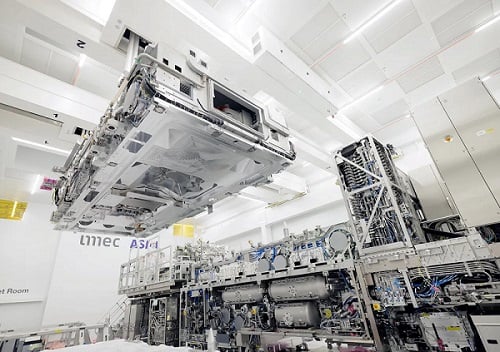
ASML and imec’s jointly-run High NA EUV Lithography Lab opened following years of preparations. The site provides access to ASML's prototype 0.55 NA EUV lithography machines, capable of printing 10 nm dense lines. Courtesy of imec.
“High NA EUV is the next milestone in optical lithography, promising the patterning of metal lines/spaces with 20 nm pitch in one single exposure and enabling next generations of DRAM chips,” said imec president and CEO Luc Van den hove. The technology is set to improve yield and reduce both cycle time and carbon emissions compared to existing multi-patterning 0.33 NA EUV systems.
Access will also be provided to the broader ecosystem of material and equipment suppliers and to imec’s High NA patterning program.
Preparations for the 0.55 NA EUV scanner and its associated infrastructure began in 2018. Since then, ASML and ZEISS developed specific solutions related to the scanner’s source, optics, lens anamorphicity, stitching, reduced depth of focus, edge placement errors, and overlay accuracy. In addition, imec, in close cooperation with its supplier network, prepared the patterning ecosystem, including the development of advanced resist and underlayer materials, photomasks, metrology and inspection techniques, anamorphic imaging strategies, optical proximity correction, and integrated patterning and etch techniques.
The preparatory work recently resulted in first exposures, showing for the first time 10 nm dense lines (20 nm pitch) printed in Veldhoven on metal oxide resists using the 0.55 NA EUV prototype scanner.
/Buyers_Guide/Imec/c22187
/Buyers_Guide/ASML/c25112