Search
Menu
PFG Precision Optics - Precision Optics 12/24 LB

ASML, University Partner Commit to $195M for Semiconductor R&D

Facebook X LinkedIn Email
ASML and the Eindhoven University of Technology (TU/Eindhoven) signed an agreement to expand their existing collaboration over the next ten years, with investment set to support semiconductor research as well as research and training in areas including plasma physics, mechatronics, optics, and AI, based on common roadmaps. The expanded collaboration will also support the establishment of a cleanroom at TU Eindhoven.

Per the agreement, ASML will invest a total of €80 million (~$87 million) into the partnership over the course of the next ten years. TU/e said that its total investment in support of the cleanroom building and to-be appointed PhD students is expected to total over €100 million.
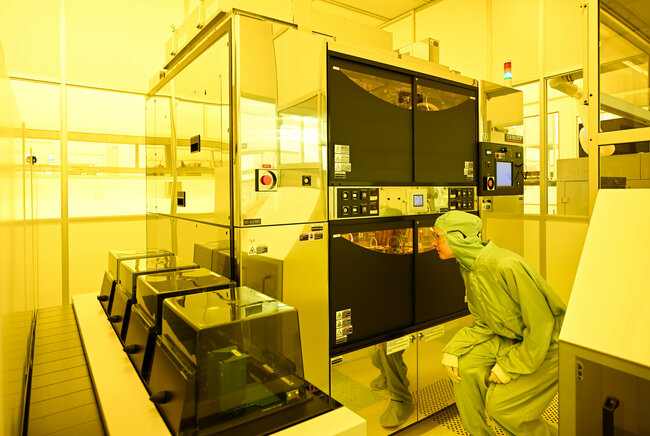
ASML and TU Eindhoven have extended their long-term collaboration. Per the agreement, the pair will invest heavily in semiconductor research and talent generation, including the establishment of a new cleanroom facility. Courtesy of Bart van Overbeeke/TU Eindhoven.
ASML and TU/Eindhoven have extended their long-term collaboration. Per the agreement, the pair will invest heavily in semiconductor research and talent generation, including the establishment of a new cleanroom facility. Courtesy of TU Eindhoven/Bart van Overbeeke
The agreement, TU Eindhoven said, is the elaboration of a memorandum of understanding signed last year by ASML and the university. The pact is in line with the €2.5 billion Project Beethoven initiative spearheaded by the government of the Netherlands and the Brainport Eindhoven region to boost semiconductor production, innovation, and talent. The collaboration also aligns with the university’s own Future Chips flagship, spurred by Project Beethoven, under which the university aims to boost the development of chip technology.
COMSOL Inc. - Find Your Best Idea MR 12/24


Published: May 2024
Glossary
integrated photonics
Integrated photonics is a field of study and technology that involves the integration of optical components, such as lasers, modulators, detectors, and waveguides, on a single chip or substrate. The goal of integrated photonics is to miniaturize and consolidate optical elements in a manner similar to the integration of electronic components on a microchip in traditional integrated circuits. Key aspects of integrated photonics include: Miniaturization: Integrated photonics aims to...
lithography
Lithography is a key process used in microfabrication and semiconductor manufacturing to create intricate patterns on the surface of substrates, typically silicon wafers. It involves the transfer of a desired pattern onto a photosensitive material called a resist, which is coated onto the substrate. The resist is then selectively exposed to light or other radiation using a mask or reticle that contains the pattern of interest. The lithography process can be broadly categorized into several...
BusinesschipscollaborationinvestmentresearchASMLPICsphotonic integrated circuitsintegrated photonicslithographyOpticseducationworkforceNetherlandsBrainport EindhovenProject BeethovenTU EindhovenEindhoven University of TechnologyEuropeIndustry News

We use cookies to improve user experience and analyze our website traffic as stated in our Privacy Policy. By using this website, you agree to the use of cookies unless you have disabled them.