Dr. Matt Novak, !%Bruker Nano Surfaces Div.%!
High-speed operation has enabled the 3-D optical microscope to transition successfully from a precision laboratory instrument to a rugged, frontline industrial tool for quality control and process-monitoring applications in diverse industries. Recent cutting-edge developments in the core technology have dramatically improved the X-Y resolution of these versatile areal measurement systems.
The 3-D optical microscope has become a versatile tool for measuring areal surface topography and texture in a wide variety of industries. A key factor in the growth of industrial applications has been hardware and software implementations that streamline and simplify its use, particularly for technician-level users.
Quantitative 3-D surface metrology – measuring surface topography as well as the size and shape of microscopic surface features – is vital to many industries. In applications including coated glossy paper, painted automobiles or molded plastic parts, surface texture affects cosmetic appearance and, hence, perceived value. But in many cases, such as with automobile engine components, medical implants or high-brightness LEDs (HB-LEDs), the surface topography can be absolutely critical to proper part functioning.
The 3-D optical microscope, based on white-light interferometry, is an ideal tool for many of these surface metrology applications, providing noncontact quantitative measurement with subnanometer resolution in the vertical (Z) axis. Moreover, this is gage-capable technology – the calibrated data are highly repeatable and reproducible, so it is compatible with most DIN, ISO and Mil-spec specifications.
The 3-D optical microscope
The 3-D optical microscope, or optical profiler, uses light waves as a high-resolution ruler or depth gauge. There are laser confocal, confocal and bright-field systems that can be implemented as 3-D microscopes; in particular, we focus on the performance advantages afforded by the use of white-light interferometry (WLI) as the foundation technology for such an instrument. Externally, such a 3-D optical microscope looks remarkably similar to a conventional optical microscope, and the device under test is placed on the sample stage. A light beam from filtered, dual HB-LED sources passes into the objective and is split into two beams by a beamsplitter. The “measurement beam” is focused onto the sample surface, while the “reference beam” is deflected onto an extremely flat, internal reference surface (Figure 1).
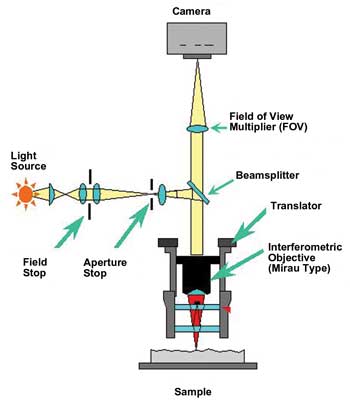
Figure 1. Schematic showing the main components of the 3-D optical microscope (Mirau configuration). Notice how the light is split to reflect off both the test surface and a reference surface and how the reflected images from these surfaces are recombined. Images courtesy of Bruker Nano Services Div.
When the reflected light from these two surfaces is recombined, optical interference creates a series of dark and light bands (called fringes) that are a direct function of the areal features of the test surface; they are analogous to elevation contours on a topographic map. Because the illumination is built from a broad-spectrum HB-LED combined beam rather than from a coherent laser, these fringes appear only when the paths of the reference beam and the measurement beams are nearly identical; i.e., the contrast of these black and white contours in any part of the image is maximized when the microscope is perfectly focused on that part of the sample.
In operation, the instrument’s computer steps the microscope through a full range of focus positions and captures the shape of these band contours on a digital camera, noting the precise focal depth at which each part of the striped image is sharpest. Onboard software then uses this data to calculate a 3-D surface map over the entire field of view (several hundred thousand, up to 1.4 million CCD pixels, depending upon the configuration) in a few seconds. The high speed of the WLI-based 3-D optical microscope resulting from this simultaneous, dense, multipixel sampling often is its most important feature in production and process monitoring applications because this supports higher-density sampling than other surface analysis methods or, indeed, other 3-D microscopes built from competing technologies.
This type of 3-D optical microscope also delivers several other important advantages, including an extremely high dynamic range, providing vertical resolution of >0.01 nm over a range of feature heights up to 10 mm. In the (horizontal) X-Y plane, the resolution depends upon the choice of microscope objective.
Besides mapping the surface areal topography and features in 3-D detail (Figure 2), system software can compute common statistical parameters such as RA and SA roughness. And measurements made with the 3-D optical microscope are noncontact and nondestructive.
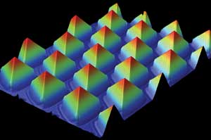
Figure 2. Typical 3-D optical microscope data using false color to indicate surface height. The sample is a patterned sapphire substrate used to form high-brightness LEDs. The data was obtained with a Bruker ContourGT-X8 PSS.
The 3-D optical microscope operates by analyzing light reflected from the test surface, so it is an excellent tool for measuring the thickness and roughness of transparent films. Here it works by analyzing the light reflected from both the top and bottom surfaces of the film.
Methods, advantages, limitations
There are numerous other surface metrology tools, each with advantages and limitations, which is why instrument manufacturers typically offer multiple modalities.
The stylus profilometer is one of the oldest surface analyzers. A contact tool, it relies on moving a fine stylus tip across the surface under test and sensing the up/down motion. Its lower cost makes it ideal for applications that can use a single linear profile (transect). But, unlike the 3-D optical microscope, it cannot be used efficiently where a 3-D surface map is required. (This can be done with a stylus, but it takes a very long time to analyze an equivalent area.)
For resolution, the atomic force microscope is widely accepted as the ultimate surface metrology tool. It senses changes in interatomic forces as a fine probe is rastered over the test surface, and it is capable of subnanometer resolution in all three dimensions. But, compared with the 3-D optical microscope, it is a relatively slow technique that is not well suited to large-area analysis.
What about other optical microscopes? The confocal microscope is widely used in biophotonics to obtain 3-D fluorescent images of living tissue at micron resolution. The technology has been adapted to surface profiling in some applications. Its main limitation, compared with the WLI-based 3-D optical microscope, is its slow speed; every X-Y-Z location must be measured sequentially.
The scanning electron microscope (SEM) can be used to obtain surface profile information at submicron resolution but requires more elaborate sample preparation and is much slower than any of these other methods. For example, in the microelectronics industry, a part is first embedded in a block of epoxy resin. After hardening, it is ground down, and the SEM beam is rastered over the exposed cross section to obtain a single linear transect profile.
In fairness to these comparisons, the one important limitation of the 3-D optical microscope should be mentioned. Specifically, the test surface must have a visible light reflectivity of at least a significant fraction of a percent to obtain a precise measurement. It cannot measure extremely dull surfaces accurately.
Packaging for industrial applications
Although the 3-D optical microscope originally was a laboratory instrument, it has been used for industrial analysis purposes for more than 20 years. It was successfully used in the early 1990s by Frito Lay to develop oriented polypropylene films with reduced defects (holes) in the metallization, leading to an order of magnitude increase in shelf life for some of its packaged snack foods.
The inherent high speed of the 3-D optical microscope makes it ideal for frontline process monitoring applications across many industries, but its successful deployment in these industries has required the development of hardware and software platforms specific to these applications. Two examples are its use in the manufacture of HB-LEDs and dynamic seals in automobiles.
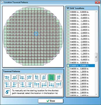
Figure 3. This screen capture from the automated software of the ContourGT-X8 PSS shows pass/fail measurements of, in this case, 260 sites on each wafer.
HB-LEDs
The 3-D optical microscope has proved both useful and versatile for process monitoring of various steps in the production of HB-LEDs, particularly those based on patterned sapphire substrates (PSS). Specifically, it can quantify the height, width and pitch of PSS features on production wafers and readily spot defective features, with greater speed and, hence, higher sampling ratios than other techniques. It also is an ideal tool for measuring surface roughness and the thickness of optically transparent films >1.5 µm in thickness.
The seamless integration of 3-D microscope process monitoring within the PSS production environment requires more than just performance and speed. Automated wafer handling, technician-level software operation, and customizable statistical analysis and archiving (Figure 3) also are absolute requirements. An example is the ContourGT-X8 PSS from Bruker, which now enables highly repeatable, high-throughput, nanometer-surface metrology of HB-LED PSS. Integrated with a Chad Industries Inc. WaferMate wafer handling system, this quality control tool supports turnkey operation for production quality assurance/quality control environments and seamless integration with automated substrate handlers. Maximum speed can be doubled by using a dual-microscope setup, as shown in Figure 4.
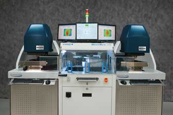
Figure 4. A dual 3-D optical microscope implementation with integrated wafer handling for the sapphire substrates speeds production testing for manufacturers of high-brightness LEDs.
Machined automotive parts
There are about 80 dynamic (usually rotary) seals in the typical automobile, according to Mercedes-Benz. These usually involve a shaft produced by some type of turning process. Residual lead (threading) causes fluid leakage, increased seal wear and shortened lifetime. Until recently, this had been measured by hanging a weight on a cotton thread draped over the shaft and observing any motion during rotation. But shafts that meet the latest government and industry standards cannot be verified by this somewhat crude process.
Some manufacturers have already switched to the 3-D optical microscope. The key developments have been software to render the measurement immune to operator influence: e.g., mounting of the shaft in the test fixture and a complex algorithm to convert observed surface features into a quantitative global lead angle (twist) measurement.
Beyond the diffraction limit
The 3-D optical microscope delivers subnanometer resolution in the Z-axis. In the X-Y plane, the instrument’s maximum limit can be affected by the microscope’s magnification and the number and size of the camera pixels, but it is ultimately limited by lens performance and diffraction. Diffraction, the natural spreading of light, is an unavoidable phenomenon from basic physics. The resolving power of a microscope also is affected by slight aberrations in its lenses. Until recently, this meant that the minimum resolvable feature size was between 300 and 500 nm, depending upon surface roughness and reflectivity.
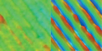
Figure 5. The increased lateral resolution delivered by AcuityXR can be readily seen in these surface maps of the same 300-nm-pitch grating without (left) and with (right) AcuityXR enabled. The vertical scale is 30 nm from blue (low) to red (high).
In theory, however, this limit can be overcome by use of novel computer algorithms combined with a very low noise threshold for measurements. In simple terms, the microscope’s computer makes use of these extremely low noise measurements in conjunction with accurate knowledge of the optical transfer function of the system. This is how the light from an ideal (zero diameter) point source is transformed into a finite-size feature in the image, and how these image features change as the microscope is adjusted through focus. In operation, the microscope’s computer inverts this function to derive sharper images from naturally blurred raw images.
This approach improves the lateral (X-Y) resolution of 3-D optical microscopes, including Bruker’s AcuityXR. Although simple in principle, this type of image correction is very difficult to implement, requiring complex algorithms that iteratively correct the images of the fringe contours until the system computer achieves the sharpest possible corrected images. The end result is an increase in lateral resolution by up to five times, as well as the ability to resolve features down to 130-nm lateral resolution. The effectiveness of this approach can be seen in Figure 5.
Meet the author
Dr. Matt Novak is market applications development manager at Bruker Nano Surfaces Div. in Tucson, Ariz.; email: [email protected].