The interaction between light source and process places demands on laser performance and parameters in applications such as semiconductor photolithography, maskless lithography and 3-D printing.
Thanks to a light – and the right – touch, a technology with its roots in printing books is today churning out chips with features too small to see, fabricating electronic devices and 3-D structures on demand. The key in every case is to have the right light source at the right price. This often means a laser, which creates structures in light-sensitive materials.
Extreme lithography
The definition of the right source at the right price varies by application. It can even change over time, thanks to advances in technology.
A case in point comes from semiconductor manufacturing, where critical feature sizes are approaching 10 nm. While semiconductor lithography is at present performed with sources operating in the deep UV at 193 nm, that wavelength isn’t short enough to economically make tomorrow’s chips. So, the industry is developing extreme-ultraviolet (EUV) sources that produce light at about 13 nm. A leading technology to do so involves a two-step process, which starts with a 10-µm wavelength pulse from a CO2 laser. This targets a rapidly moving tin droplet.

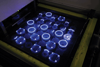
Directed UV laser reacting with the surface of the resin to cure the designs. The blue glow is from the UV laser – directed by dynamic mirrors, the laser cures resin layer by layer to build 3-D designs. Photo courtesy of Stratasys Direct Manufacturing.
“The pulse heats the tin from a liquid into a vapor and then starts superheating the vapor, such that the electrons start shedding from each individual atom,” said David Brandt, senior director of EUV product management at San Diego-based Cymer Inc. The subsidiary of semiconductor tool maker ASML produces advanced lithography light sources.
As a result of superheating, the tin turns into a plasma and emits a strong line at 13.5 nm. That radiation is collected, focused and then used for EUV lithography.

High-resolution, high-aspect-ratio, direct-write laser lithography on the thick resist. Photo courtesy of Heidelberg Instruments.
Over the past few years, significant technological strides have upped the efficiency and economics of the process. For instance, the tin vaporization is now done with a double pulse. The first pulse is gentler and conditions the droplet, transforming it from a sphere into a larger diameter disk. That improves the absorption efficiency of the second pulse, which is more powerful. Amplifiers have been added, as well, both to increase the laser power and to stabilize its output.
Another improvement is the switch to all reflective optics to eliminate performance-robbing thermal effects.
The result of these and other changes has been that power at EUV wavelengths has gone from 10 W to 80 W in the field. Higher levels have been demonstrated internally, according to Brandt.

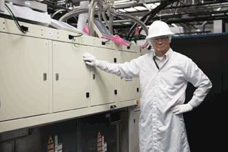
Lasers target a tin drop, creating a plasma and an EUV 13.5-nm light source needed for future semiconductor chips. Photo courtesy of Cymer.
Gigaphoton Inc. of Oyama, Japan, another advanced lithography manufacturer, has publicly stated it will achieve a 250-W prototype by year’s end. That power level is what chip makers have said they need, but getting there will require pushing laser parameters, Brandt said. For instance, the repetition rate of the CO2 laser will probably have to double from the current 50,000 Hz.
In the future, the source makers might be able to borrow from advances made elsewhere. “The closest technology out there is laser fusion,” Brandt said, wherein the target is water and not tin. Another difference is that laser fusion uses 1-µm YAG lasers. In both cases, lasers blast a tiny droplet, which requires synchronization. As a result, the technology developed could someday play a role in making chips.
Achieving tight control
EUV may be the lithography source of the future, but today’s 193-nm sources will be used for years to come. The lithography tools are asked to produce features with critical dimensions as low as 14 nm; that’s more than 10 times smaller than the wavelength, which means the imaging is happening well below the diffraction limit.
This is accomplished through double- and multipatterning. In these techniques, successive lower density subpatterns are imaged, sidestepping diffraction constraints. However, because exposures overlap, the lithography process has to be increasingly stable, while at the same time becoming less expensive.
Cymer is attempting to achieve that difficult combination, in part by focusing on three key source metrics: energy, wavelength and bandwidth. The last is the measure of the output spread around the nominal wavelength, and it plays a role in optimization.
“The narrower the bandwidth, the better you can design your imaging and achieve better contrast,” said Dr. Ted Cacouris, director of deep-ultraviolet product marketing at Cymer in San Diego.
In February 2015, Cymer announced a laser source with 95 percent of its output falling within 300 femtometers of the nominal center point. Achieving that tight an output from excimer lasers, which are naturally somewhat variable, requires feedback and advanced control. For this, the company uses proprietary technology.
It will be some time before EUV takes over, as it is still under development. What’s more, it’s a radically different lithography, requiring changes to optics, resists, masks and sources. The multibillion-dollar semiconductor industry may put off the lithography switch until forced by physics and economics. Consequently, the demands on deep-ultraviolet lithography and lasers should ratchet up.

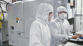
In semiconductor manufacturing, 193-nm wavelength deep-ultraviolet laser sources (white box behind engineers) help fabricate chips with feature sizes approaching 14 nm, which requires a tightly controlled source. Photo courtesy of Cymer.
“We, as a company, continue to invest in deep-ultraviolet. There’s significant work that needs to happen,” Cacouris said.
Maskless lithography
Maskless lithography is another application benefitting from the right source at the right price. As the name implies, this technology uses a beam to write directly into photoresist, making it possible to fabricate micron-scale structures in flat panels, electronics and elsewhere. An advantage of this approach is that it covers large areas. Another is that prototyping and development are easier, since layout changes can be made quickly.
Germany-based Heidelberg Instruments Mikrotechnik GmbH makes maskless lithography products that can expose areas as small as a few millimeters across, up to about 1.4 meters on a side, said Alexander Forozan, vice president of global sales and business development. Lasers are the light engines that make everything work.
“Lasers are modulated to create structures on the surface of the photoresist, or other photosensitive material, to create micro- and nanostructures. Important laser characteristics are wavelength, stability, power, cost and lifetime,” Forozan said.
The last three characteristics play a role in the economics of maskless lithography. More power, for instance, translates into higher throughput and greater productivity. A longer lifetime would mean less downtime and reduced operating expenses.
Stability and wavelength factor into system performance. A more stable laser means that features have less variation, while wavelength is critical to the process of polymerization that turns photoresist solid. In the case of Heidelberg Instruments, the sources are 532-nm green diode lasers operating at 100 mW, 405-nm diode lasers operating at up to 300 mW and 355-nm dual-pumped solid-state lasers operating at up to 10 W. The laser choice depends on the lithography process and the resist, Forozan said. Those wavelengths help determine the feature size, which today is about 500 nm.
As for what’s needed in the future, laser improvements are vital, according to Forozan. “Price per watt is very crucial, as well as the lifetime. We need to increase the throughput and at the same time reduce the running costs.”
Into the third dimension
For a final look at the impact of lasers on lithography and vice versa, consider stereolithography. Here, a laser source activates a photopolymer, allowing the building up layer by layer of a 3-D structure. It’s a technology that lies at the heart of many 3-D printers.

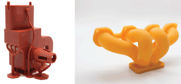
Lasers make it possible to produce intricate 3-D structures. Photo courtesy of Full Spectrum Laser/FSL3D.
Andrew Boggeri, lead mechanical engineer at Full Spectrum Laser LLC and its subsidiary FSL3D of Las Vegas, noted that the field was transformed with the advent of inexpensive 405-nm lasers. That made it possible to take advantage of resins that required near-ultraviolet for activation. Going still deeper in the UV to 365 nm or so would be helpful for various reasons, according to Boggeri.
“What would we see? A throughput increase is one because the catalyst is more responsive to a deeper UV,” he said.
It also would mean that different and higher performance materials could be produced. Strength would be greater and total transparency achievable, making it possible, for instance, to make plastic optics. The problem is that the laser sources currently available at 365 nm and nearby wavelengths are too costly for use on inexpensive industrial or consumer products. Prices are falling though, and if that trend continues, it will eventually alter the equation.
Andrew Graves is an additive manufacturing engineer at Stratasys Direct Inc., a rapid prototyping manufacturing service based in Valencia, Calif. The company employs solid state lasers operating at 355 nm, using a resin tuned to that wavelength. The resulting parts have what Graves termed “beautiful sidewalls and very good feature definition.”
However, achieving that performance on a consistent basis entails getting rapid and accurate wavelength data, as well as information on beam position, shape, size and power. That will be important in any successful 3-D printing system because it forms the basis for closed-loop laser control.
As Graves said, “You need to know what [the laser is] doing, and if it’s not doing something, you have to compensate for it. You have to have the means to measure those things.”