Laser achievements in the laboratory this past year ranged from some of the smallest ever made to some of the largest, from the debut of the world’s first hard x-ray free-electron laser to creation of the most powerful light ray yet by a solid-state laser.
A major laser milestone for 2009 was the announcement that a facility that aims to harness the power of stars and giant planets was finally ready to be put into action.
With its 192 giant laser beams, the National Ignition Facility (NIF), located at Lawrence Livermore National Laboratory outside of San Francisco, is the world’s largest and highest-energy laser. It will deliver at least 60 times more energy than any previous laser system.
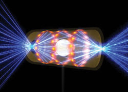
This artist's rendering shows a NIF target pellet inside a hohlraum capsule with laser beams entering through openings on either end. The beams compress and heat the target to the necessary conditions for nuclear fusion to occur. Ignition experiments on NIF will be the culmination of more than 30 years of inertial confinement fusion research and development, opening the door to exploration of previously inaccessible physical regimes. Credit is given to Lawrence Livermore National Security LLC, Lawrence Livermore National Laboratory, and the US Department of Energy, under whose auspices this work was performed.
NIF was built as a part of the National Nuclear Security Administration’s (NNSA) program to ensure the safety, security and effectiveness of the nuclear weapons stockpile without underground testing.
The facility, dedicated May 29, will begin experiments this year that focus the energy of all its ultraviolet laser beams – nearly 2 million joules – for a few billionths of a second onto a hydrogen fuel-filled gold target the size of a BB called a hohlraum. NIF’s goal is essentially to create the power of a star in the lab to advance fusion energy technology.
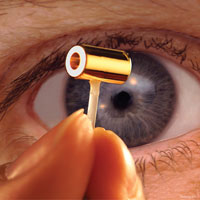
A National Ignition Facility (NIF) hohlraum. The hohlraum cylinder, which contains the fusion fuel capsule, is just a few millimeters wide, about the size of a pencil eraser, with beam entrance holes at either end. The fuel capsule is the size of a small pea. Credit is given to Lawrence Livermore National Security LLC, Lawrence Livermore National Laboratory, and the US Department of Energy, under whose auspices this work was performed.
“The tiny star created is about the diameter of one hair,” said Dr. Peter J.K. “Jeff” Wisoff, associate director of NIF and Photon Science, during a session at the Frontiers in Optics Conference in San Jose, Calif., in October. The implosion of the fuel pellet is equivalent to the energy created by the explosion “of a hand grenade or two,” he said. The goal is to release more energy than the laser energy expended to create it.
People joke that “fusion is 50 years away, no matter when you ask,” NIF Director Edward Moses said during a plenary speech at the Conference on Lasers and Electro-Optics (CLEO), held in Baltimore last June. “But NIF could make it happen in two years.”
Wisoff said NIF’s two goals are to “start ignition experiments in 2010 and to demonstrate a reliable and repeatable ignition platform so we can become a national user facility.”
In November, NNSA announced that recent NIF tests showed that its laser beams can be delivered effectively and are capable of creating sufficient x-ray energy to drive fuel implosion, an important step that shows NIF can fulfill a key requirement of the fusion process. The Laboratory for Laser Energetics also presented results showing the most compressed fusion capsules to date.
Northrop Grumman Corp. of Redondo Beach, Calif., announced in March that it had produced the most powerful light ray yet created by a solid-state laser, measured at more than 105 kW. The achievements included a turn-on time of <1 s and continuous operating time of 5 min with very good efficiency and beam quality, the company said. The weapon system was developed for Phase 3 of the US military’s Joint High Power Solid State Laser program.
“This achievement is particularly important because the 100-kW threshold has been viewed traditionally as a proof of principle for ‘weapons grade’ power levels for high-energy lasers,” said Dan Wildt, vice president of Directed Energy Systems for Northrop Grumman’s Aerospace Systems sector. “In fact, many militarily useful effects can be achieved by laser weapons of 25 kW or 50 kW, provided this energy is transmitted with good beam quality, as our system does. With this milestone, we have far exceeded those needs.”
The Linac Coherent Light Source (LCLS) at SLAC National Accelerator Lab in Menlo Park, Calif., the world’s first hard x-ray free-electron laser, produced its first laser light last April.
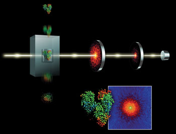
The Linac Coherent Light Source (LCLS) will create 3-D holographic images of single molecules using ultrafast pulses of very intense hard x-rays.
“This is the most difficult light source that has ever been turned on,” said LCLS construction project director John N. Galayda.
Instead of using mirrored cavities to amplify light, the LCLS creates light using free-flying electrons in a vacuum. It uses the final third of SLAC’s two-mile linear accelerator to drive electrons to high energy and through an array of undulator magnets that steer the electrons rapidly back and forth, generating a brilliant beam of coordinated x-rays.
The LCLS can resolve detail the size of atoms at 10 billion times the brightness of any other man-made x-ray source.

The LCLS creates intense pulses of hard x-rays using tightly packed bunches of electrons traveling through arrays of undulator magnets. Shown here is an artists’s conception of an electron pulse between the alternating poles of the undulator. Images courtesy of LCLS.
“No one has ever had access to this kind of light before,” said LCLS Director Jo Stöhr.
By 2013, the LCLS is expected to provide groundbreaking research in physics, structural biology, energy science and chemistry, among others, once all six of its scientific instruments are online. Early experiments already have provided new insights into the fundamentals of atomic physics and have successfully proved the machine’s ability to control and manipulate the underlying properties of atoms and molecules.
Last fall, researchers used the LCLS’ strobelike pulses to strip neon atoms of all their electrons. The extreme brightness of the laser beam also allowed them to study two-photon ionization, an event where two photons pool their energy to eject a single electron from an atom.
The Fraunhofer Institute for Laser Technology (ILT) unveiled the world’s most powerful ultrashort-pulse laser during Laser World of Photonics 2009 in Munich in June. The femtosecond laser, which comprises a single-pass amplifier with four mirrors and one laser crystal, has an average output of more than 400 W and holds the record for average output among lasers with pulse durations of <1 ps.
The Fraunhofer researchers said they achieved the breakthrough by reinterpreting the InnoSlab technology that has been under development at the institute for more than 10 years. The technology already forms the basis for many nano- and picosecond laser systems currently in industrial use.
Many notable achievements in laser research also were accomplished in the past 12 months or so in university campus labs.
In late December 2008, researchers at Princeton University’s Mid-Infrared Technologies for Health and the Environment (MIRTHE) center announced their discovery that a quantum cascade laser (QCL) can generate a second beam with very unusual properties, a feat that could lead to lasers that operate more efficiently and at higher temperatures than existing devices, for applications including environmental monitoring and medical diagnostics.
“This discovery provides a new insight into the physics of lasers,” said Claire F. Gmachl, who led the study. Gmachl, an electrical engineer at Princeton University, is the director of MIRTHE.
In January 2009, Harvard University’s Federico Capasso led a study that revealed for the first time a measurable, repulsive Casimir force that could be tailored for a wide range of new nanotechnology applications.
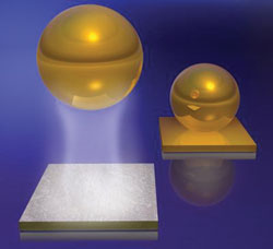
An artist's rendition of how the repulsive Casimir-Lifshitz force between suitable materials in a fluid can be used to quantum mechanically levitate a small object of density greater than the liquid (Figures are not drawn to scale). Foreground: a gold sphere, immersed in bromobenzene, levitates above a silica plate. Background: when the plate is replaced by one of gold, levitation is impossible because the Casimir-Lifshitz force is always attractive between identical materials. Image courtesy of the lab of Federico Capasso, Harvard School of Engineering and Applied Sciences.
Attractive Casimir forces can limit the ultimate miniaturization of microelectromechanical systems because the attractive forces may push together moving parts and render them inoperable, an effect known as stiction, or static friction.
At the nanoscale, these quantum forces compel metallic surfaces placed very close to each other in a vacuum, in fluid or in air-filled space to attract. Capasso and his group discovered that replacing one of the two metallic surfaces immersed in a fluid with one made of silica switched the force between them from attractive to repulsive.
“Repulsive Casimir forces are of great interest since they can be used in new ultrasensitive force and torque sensors to levitate an object immersed in a fluid at nanometric distances above a surface. Further, these objects are free to rotate or translate relative to each other with minimal static friction because their surfaces never come into direct contact,” Capasso said.

Last April, Capasso and applied scientists at the Harvard School of Engineering and Applied Sciences, working in collaboration with researchers from Hamamatsu Photonics KK in Japan, sculpted a metallic structure, dubbed a plasmonic polarizer, directly onto the facet of a QCL. They used the device to demonstrate that the direction of oscillation of the emitted radiation, or polarization, can be designed and controlled at will for new applications in photonics and communications.
“The novelty of our approach is that, instead of being conducted externally, which requires bulky and expensive optical components, manipulation of the beam polarization is achieved by directly integrating the polarizer on the laser facet. This compact solution is applicable to semiconductor lasers and other solid-state lasers, all the way from communication wavelengths to the mid-infrared and terahertz spectrum,” Capasso said.
The team controlled the state of polarization by generating both linearly polarized light along an arbitrary direction and circularly polarized light.
Also in April, engineers at the Centre of Molecular Materials for Photonics and Electronics (CMMPE) at the University of Cambridge in the UK announced their development of self-organizing, tiny, highly tunable liquid crystal lasers that could soon be used in displays, in medical diagnostics and in sensors because they could be produced at a fraction of the cost of other display technologies.
The new technology uses liquid crystals in concert with a single, laser-based light source. Typically, lasers have two mirrors, and light bounces back and forth between them, but liquid crystal lasers do not use mirrors because the optical cavity is defined by the pitch (the length of one complete twist of a crystal). By controlling the degree of twist, the researchers discovered how to tune the output wavelength of the liquid crystal lasers.
“These polychromatic lasers are capable of narrowband emission at any wavelength in the spectrum from near ultraviolet to near-infrared,” said professor Harry J. Coles, director of the CMMPE. “When added to the ability to produce 100 x 100 arrays of such lasers, in tens of micron spots and, indeed, 10-micron cavity lengths, with very high conversion efficiencies of up to 60 to 70 percent, they open up a range of novel applications.
“Currently, the lasers use a single-pulsed solid-state miniature benchtop laser to pump the lenslet arrays, but we anticipate that this will be replaced by a miniature blue laser diode in the very near future,” Coles said in April. “The [liquid crystal] lasers have already demonstrated quasi-CW working at a 10-kHz repetition rate and so, to the human eye, appear to be a continuous ‘any wavelength’ laser.”
In July, a collaboration between researchers at Arizona State University and Technical University of Eindhoven in the Netherlands resulted in advances in overcoming previous limitations on how small lasers can be made.
“This is the first time that anyone has shown that this limit to the size of nanolasers can be broken,” said ASU team leader Cun-Zheng Ning. “Beating this limit is significant. It opens up diverse possibilities for improving integrated communications devices, single-molecule detection and medical imaging.”
The theory of diffraction limit – a property associated with any wave, such as a beam of light – had said that the size of a laser in any one dimension (such as thickness) was thought to be limited to one-half of the wavelength involved.
But the ASU and Eindhoven research teams showed that there are ways around this supposed limit, including using a combination of semiconductors and metals such as gold and silver.
“It turns out that the electrons excited in metals can help you confine a light in a laser to sizes smaller than that required by the diffraction limit,” Ning said. “Eventually, we were able to make a laser as thin as about one-quarter of the wavelength or smaller, as opposed to one-half.”
In August, a team at the University of California, Berkeley, said that it had broken new ground in optics by not only successfully squeezing light into an incredibly tight space but by achieving laser action in finding a novel way to keep that light energy from dissipating as it moved. The researchers’ new type of nanoscale laser concentrates light into an area one-hundredth the size of the smallest spot that can be produced by a conventional laser – a space smaller than a single protein molecule.
“This work shatters traditional notions of laser limits and makes a major advance toward applications in the biomedical, communications and computing fields,” said Xiang Zhang, professor of mechanical engineering, director of UC Berkeley’s Nanoscale Science and Engineering Center, and head of the research team behind the work.
A technology that uses man-made diamonds to enhance the power and capabilities of lasers was announced in September by a research group in Australia.
The team’s Raman laser has applications that range from defense technologies and trace gas detectors to medical devices and satellite mapping of greenhouse gases.
Existing Raman lasers typically use crystals of silicon, barium nitrate or metal tungstate to amplify light created by a pump laser. Compared with these materials, diamond has a higher optical gain as well as a greater thermal conductivity, making it ideal for high-power applications such as in defense, gas detection, medical devices and environmental monitoring. Diamond crystals also can be made to generate a wider variety of wavelengths of light, each of which has its own applications – from ultraviolet to far-infrared.
Also in August, researchers at Purdue University in West Lafayette, Ind., at Norfolk State University in Virginia and at Cornell University in Ithaca, N.Y., announced that they had created the world’s tiniest laser, dubbed the “spaser.” Because traditional lasers cannot be made small enough to integrate onto electronic chips, the scientists created the tiny spasers by harnessing surface plasmons instead of photons.
The nanolasers were spheres 44 nm in diameter – more than 1 million could fit inside a red blood cell. The spheres were fabricated at Cornell, with Norfolk State and Purdue performing the optical characterization needed to determine whether the devices behave as lasers.
The device – the first of its kind to emit visible light – represents a critical component for possible future technologies, including superfast computers that use light instead of electrons to process information, and advanced sensors and imaging, the researchers said.
In late November, Capasso was back in the news as part of an international team of applied scientists who had demonstrated compact multibeam and multiwavelength lasers emitting in the infrared.
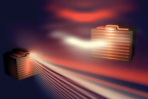
An example of a compact, multibeam and multiwavelength laser. Unlike typical semiconductor lasers that emit single beams of light pointing in a single, well-defined direction, the multibeam laser can use versatile light sources. The innovation has potential use in applications related to remote chemical sensing, pollution monitoring, optical wireless and interferometry, and it was developed by a team of applied scientists from the Harvard School of Engineering and Applied Sciences, Hamamatsu Photonics and ETH Zürich. Courtesy of the lab of Federico Capasso, Harvard School of Engineering and Applied Sciences.
In one of the prototypes demonstrated by the team, the new laser emits several highly directional beams with the same wavelength near 8 µm, a function very useful for interferometry, which requires two coherent beams: a probe and a reference. The probe beam interacts with a sample and recombines with the reference beam to reveal optical properties of the sample. A second type of laser emits multiple small divergence beams with different wavelengths – 9.3 and 10.5 µm – into different directions.
Although the researchers demonstrated the idea using mid-infrared semiconductor lasers emitting wavelengths in the 8- to 10-µm range, the concept can be generalized to lasers emitting other wavelengths in the near-infrared and terahertz spectrum, or to passive optical components such as optical fibers. For example, nano-structures can be patterned on the facet of optical fibers to help build microendoscopes for in vivo diagnostics, they said.
In early December, scientists led by Qing Hu, professor of electrical engineering at MIT’s Research Laboratory of Electronics in Cambridge, described the first practical method for tuning terahertz QCLs, stating that their method is a fundamentally new approach to laser tuning that could have implications for other emerging technologies.
His new tuning technique requires a type of QCL called a wire laser, in which the wavelength of the transverse mode – the width of the one big undulation – is actually greater than the width of the laser itself.
Bringing a block of another material close enough to the laser deforms the transverse mode, which, in turn, changes the wavelength of the emitted light. In experiments, Hu and his colleagues found that a metal block shortened the wavelength of the light, while a silicon block lengthened it. Varying the proximity of the blocks also varies the extent of the shift.
Hu’s group used a mechanical lever to bring a block of either silicon or metal close to a QCL from a single direction. But it has designed and is now building chips that would use electronically controlled microelectromechanical devices to bring the silicon and metal blocks in from different directions, giving the laser a precise and continuous tuning range from short to long wavelengths.