A new laser tool improves solar cell manufacturing output and lowers dollar per watt costs.
Dave Clark, Newport Corp./Spectra-Physics
Photovoltaic (PV) solar cells have been around for more than 50 years now, enjoying initial commercial success in familiar applications such as powering satellites in space and, later on, digital calculators and other portable devices. Since the early days, scientists have dreamed of the widespread deployment of photovoltaic cells on rooftops, in deserts and in fields to harness the power of the sun and produce “endless” amounts of cheap, clean electricity. Unfortunately, significant challenges have made progress disappointingly slow.
The “holy grail” for the PV scientist is to produce devices with a low enough cost and high enough conversion efficiency to be competitive with traditional methods of generating electricity. The drive to achieve this has created considerable interest in a range of emerging laser-based manufacturing processes. One of the most promising is laser doping of selective emitters.
Improving front side contacts
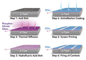
Key areas in traditional wafer-based crystalline-silicon solar cells requiring major improvement are the quality and functionality of front and rear surface contacts. The process currently employed is detailed in Figure 1. The traditional screen-printed silicon solar cell manufacturing process has six steps:

Figure 1. The traditional screen-printed silicon solar cell manufacturing process consists of six steps. Images courtesy of Newport Corp./Spectra-Physics.
Step 1: An acid etch of the p-type wafer is used to remove saw damage and to texture the surface, improving the absorption of incident light.
Step 2: Thermal diffusion of phosphorus doping in a furnace with POCl3 gas creates the lightly doped n+ emitter region.
Step 3: The hydrofluoric acid etch process removes the phosphor-silicate glass.
Step 4: Deposition of an antireflection thin-film coating of silicon nitride (SiNx) on the front surface.
Step 5: Screen printing of the front surface contacts.
Step 6: Heating or “firing” the contacts melts them through the thin insulating layer of SiNx to make contact with the underlying n+ silicon layer.
The existing method of contact formation presents a number of issues. First, the conventional screen-printed metal grid lines and bus bars are quite wide in cross section, around 120 μm. They also have a poor aspect ratio – typically only 13 μm in height. These opaque metal lines obscure the active areas of the silicon cell beneath, causing a reduction in fill factor and what is commonly referred to as “shading losses.” This shading effectively reduces the cell efficiency. The second issue is that the firing process does not usually result in optimal electrical contact between the metal of the grid lines and the underlying silicon. This leads to contact over only a small percentage of the area shaded by the metal line and, given the size of the grid lines, a relatively high series resistance. The third concern: The n+ doping profile cannot be easily tailored to create low-resistance contact areas directly underneath the metal contacts, so a trade-off must be made by applying a uniform concentration of dopant across the entire cell surface.
To improve upon the traditional screen-printed front contacts, Martin Green’s group at the University of New South Wales in Australia devised the laser-grooved buried contact solar cell. They employed a laser to ablate the U- or V-shape grooves that subsequently could be cleaned, doped and plated to create more optimal contacts. This was the basis of the BP Solar Saturn cell, which enjoyed many years of production success.

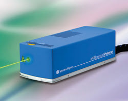
Figure 2. Newport Corp./Spectra-Physics’ Millennia Prime is a field-proven laser and is ideally suited for applications involving laser doping of selective emitters.
However, the laser-grooved buried contact solar cell required high-quality silicon substrates and employed multiple additional process steps in its manufacture; the resulting high unit costs led to its eventual demise. Sadly, BP Solar was forced to end production of this elegant laser-enabled solar cell and recently closed its plant in Madrid, Spain.
A simple method for fabricating much finer front surface contacts with high aspect ratios and excellent contact to the underlying silicon and strongly doped regions directly beneath them was needed. The University of New South Wales scientists again were at the forefront of solving this problem with their more recent work in the area of laser doping of selective emitters. Using lasers in these new solar cell designs promises to offer significantly better performance over the existing screen-printed technologies, and yet the new cells are relatively simple and inexpensive to implement in existing production lines.
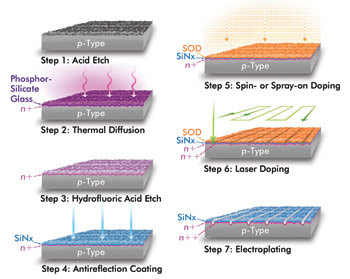
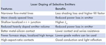
The basic process steps for manufacturing the front side contacts for the new design are shown in Figure 3. This technology employs a larger number of much narrower metal finger contacts with heavily doped regions of n++ beneath each individual contact. The features and benefits are detailed in the table.

Figure 3. Laser doping of selective emitters involves seven process steps.
There are seven steps for laser doping of selective emitters. Steps 1 through 4 are the same as for the traditional screen-printed silicon solar cell manufacturing process.
Step 5: A spun-on or spray-on thin, uniform coating of n-type dopant (SOD).
Step 6: Laser doping: A laser simultaneously ablates the SiNx and melts the underlying silicon. Phosphor almost instantaneously migrates into silicon while it is in liquid phase to create a shallow, highly doped n++ region.
Step 7: Wash off SOD, and electroplate to create self-aligned contacts.
This new, elegant process has been shown to increase cell efficiencies for both mono- and multicrystalline cells by up to as much as 2 percent in absolute terms. This is a 10 percent improvement over more traditional screen-printed cells. Understandably, this has created a huge amount of interest in the industry.
Most of the early process development work on laser doping used Q-switched lasers, often in the green, but limitations on process speeds and quality confined this work to the lab. Thanks to advances in the past few years, mode-locked UV lasers are now being used with some success; they provide a small spot size and faster scan speeds than Q-switched lasers because of their higher repetition rates. However, there are important challenges in integrating such high-power UV mode-locked lasers into production tools. In particular, UV optics and lasers are inherently less robust than green or infrared lasers and thus much more expensive. The industry’s high cell-throughput requirements are currently driving manufacturers to look at a third option – namely high-power, continuous-wave (CW) green lasers. Newport Corp.’s Spectra-Physics Div.’s CW green laser, the Millennia Prime, has proved ideal for laser doping of selective emitter applications. Recent lab results have shown that this type of laser can scan the entire cell at up to two to five times the speed of existing methods. It also can be integrated into a lower cost and more robust tool with much higher cell throughput, providing a distinct advantage to solar cell manufacturers.
 Laser tool considerations
In the solar cell industry, each tool in the manufacturing line must be highly reliable, produce consistently high yields and have a throughput that is balanced to match the rest of the line. In the typical 30-MW production line, this translates to 1100 to 1200 wafers per hour and tools operating 24/7 in factories around the globe. It is critical, therefore, that laser tools be extremely robust and able to process and handle wafers with very low breakage at these high- throughput rates. These requirements create a huge challenge considering that the newest wafers are typically only 200 μm thick and that the takt times are just a few seconds. Additionally, there are significant optical engine and scanner design challenges in processing reliably across the larger wafers without making the production tool highly complex and costly.
Meet the author
Dave Clark is senior director of strategic marketing, photovoltaics, at Newport Corp./Spectra-Physics in Mountain View, Calif.; e-mail: [email protected].