
Nanolasers grown on silicon surface
Nanolasers now can be grown directly onto
a silicon surface, an achievement that could lead to a new class of faster, more
efficient microprocessors, as well as to powerful biochemical sensors that use optoelectronic
chips.
The results are expected to affect a number of scientific fields,
including materials science, transistor technology, laser science, optoelectronics
and optical physics, according to a group of engineers at the University of California.
Their work was published online Feb. 6, 2011, in
Nature Photonics (doi: 10.1038/nphoton.2010.315).
In search of a better way to harness light particles so that they
may carry more data than electrical signals can, the researchers turned to a class
of materials known as III-V semiconductors to create light-based components such
as LEDs and lasers. Silicon, the foundation material for most modern electronics,
is deficient at generating light.
They found that marrying III-V with silicon to create a single
optoelectronic chip is problematic. Although it can be done, the material can get
damaged in the process because the growth of the semiconductors traditionally has
involved high temperatures of more than 700 °C.
The researchers found a way to grow nanopillars made of indium
gallium arsenide, a III-V material, onto a silicon surface at a relatively cooler
temperature of 400 °C. They used metallorganic chemical vapor deposition to
grow the nanopillars on the silicon. The technique has the potential to be mass
manufactured since systems used to make thin-film solar cells and LEDs are already
commercially available.
“Working at nanoscale levels has enabled us to grow high-quality
III-V materials at low temperatures such that silicon electronics can retain their
functionality,” said Roger Chen, University of California, Berkeley, graduate
student in electrical engineering and computer sciences.
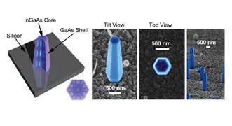
Shown are a schematic (left) and various scanning electron microscope images of nanolasers grown directly on
a silicon surface. The achievement could lead to a new class of optoelectronic chips.
Courtesy of Connie Chang-Hasnain Group, UC Berkeley.
With the ability to generate near-IR laser light, the nanopillar
can be packed into small spaces while consuming very little energy. Growing nanolasers
directly onto silicon could lead to highly efficient silicon photonics. In addition,
the technique may provide a new avenue for engineering on-chip nanophotonic devices,
including lasers, photodetectors, modulators and solar cells, Chen said.
The research was supported by DARPA and a US Department of Defense
National Security Science and Engineering Faculty fellowship.
LATEST NEWS
