Selecting CCDs for Raman Spectroscopy
John Gilmore, Hamamatsu Corp.
Raman spectroscopy is a well-known technique
used to identify materials and chemicals. Until the 1980s, most Raman instruments
used dedicated monochromators with photomultiplier tube (PMT) detectors.
1 These
early systems enjoyed the high sensitivity that a PMT provides but lacked versatility
and red response (700- to 1000-nm region).
Today the Raman market is dominated by CCD detectors with versatile
grating and high sensitivity in the red and near-IR regions. This article will explain
how to select a CCD detector for Raman spectroscopy, focusing primarily on relevant
CCD device parameters, their trade-offs and why they are important to Raman spectroscopy.
The most recent trend is making small, portable handheld Raman
instruments to measure such things as biohazardous materials, diseases and bacteria.
The demand for high-performance sensors and instrumentation in this application
is driving the evolution of new product development. Instrument manufacturers require
image sensors such as CCDs to have low noise, high sensitivity, low etaloning and
excellent linearity characteristics.
Noise
Because this new generation of handheld Raman instruments is often
battery-powered, cooling the image sensor is not a viable solution for noise reduction.
There are only a handful of CCD manufacturers in the world capable of producing
noncooled image sensors with intrinsically low noise. Manufacturers who own a foundry
tend to have better quality control over the CCD manufacturing process compared
with those who outsource. Having such a foundry enables optimizing the wafer processing
conditions to reduce the dark current. This is very important for Raman spectroscopy.
Speed
The topic of operating speed can be viewed from two perspectives:
instrument and CCD sensor readout. The two topics can be confusing because the terminology
for each opposes the other. And because the optical signal impinging on the CCD
surface is extremely weak, people generally are not concerned about fast CCD readout
speed.
Reading out the CCD sensor in a matter of a few milliseconds to
tens of milliseconds is perfectly acceptable for most applications. The tendency
is to increase the integration time – on the order of a fraction of a second
to several seconds – to improve the signal-to-noise ratio. Operating the CCD
at high pixel frequencies, or high readout speed, will be counterproductive in terms
of increased readout noise, increased power consumption and self-heating of the
CCD chip, thus increasing the CCD dark signal.
The rate at which Raman spectral data is acquired is very important
for some applications, as stated earlier. If all other variables are held constant,
spectral data can be acquired at twice the speed by using a back-thinned CCD with
double the quantum efficiency of conventional CCDs. This means that a handheld instrument
can perform material analyses faster, an important benefit for security applications.
Quantum efficiency
Raman signal – number of photons – typically is very
weak, and detectors must capture every available photon to maximize the signal-to-noise
ratio. The optical signal for a classical Raman measurement – not surface-enhanced
– is extremely low: Only 0.001 percent of the excitation source is converted
into Raman signal. This means that the Raman measurement system must be capable
of detecting weak optical signals, down to the level of tens of photons.

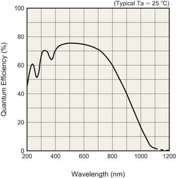
Figure 1. Quantum efficiency curve of a conventional back-thinned
CCD (BT-CCD). Images courtesy of Hamamatsu Corp. Ta = ambient temperature.
Back-thinned CCDs (BT-CCDs) are well suited for such low light
detection because their quantum efficiency (QE) reaches 90 percent at the peak wavelength
(Figure 1). Such devices have high QE in the UV and visible regions because the
incident light interacts directly with the sensor’s active region.
Making their transition from R&D to mass production, near-IR-enhanced
BT-CCDs also are proving to be a benefit for Raman spectroscopy. Laser treatment
of the BT-CCD can further increase the QE in the red and near-IR regions (Figure
2). The advantage of higher QE is improved signal-to-noise ratio. With this new
technology, instrument designers can double the signal-to-noise ratio at 800 nm.
Figure 2. Quantum efficiency curves of a front-illuminated CCD, BT-CCD
(conventional type) and IR-enhanced BT-CCD.
Etaloning
The drawback to a back-thinned CCD is etaloning. As light passes
through the thinned region (10 to 20 μm thick), a small percentage of the light
hits structures, or layers, near the front side and reflects back into the active
region, generating electrons (signal). This is particularly noticeable in the red
and near-IR regions. The reflected signal creates a fringe pattern in the spectral
response (Figure 3).
The best technique to reduce etaloning is to create irregular
patterns at the origin of reflection, preventing the light from reflecting back
into the active region. By employing such patterns, Hamamatsu can reduce the etaloning
by a factor of five. Reducing etaloning is of great benefit to the end user because
the interference pattern would otherwise mask the actual spectral signature of the
sample, making identification of the sample impossible.
Figure 3. Comparison of etaloning in a conventional BT-CCD and a BT-CCD with low etaloning.
Linearity
Some applications of Raman spectroscopy require the ability to
measure concentrations of samples. In such cases, it is necessary for the Raman
instrument to have good linearity. Linearity of the CCD is governed by the design
of the on-chip floating diffusion amplifier. Linearity often is not written as a
specification, so be sure to contact CCD manufacturers and request the data.
As a common practice, many instrument designers will write algorithms
to compensate for nonlinearity. The task of linearity correction is made easier
if you select a CCD that inherently has a good linear response.
Electronic circuitry
Equally important is the electronics design of the CCD readout
circuitry and clock drivers. The highly optimized CCD sensors described previously
are of no value without proper readout and interface electronics. Electronics designers
have the option to use discrete components – amplifiers, correlated double
sampling and analog-to-digital converters – or an “all in one”
approach with an analog front-end (AFE) device. The trade-off is simple. AFEs offer
simple implementation with low power consumption and compact size. On the other
hand, discrete circuit designs offer the lowest readout noise (as much as 30 percent
lower than an AFE design), but are more complicated to implement and often require
an experienced low-noise analog design engineer.
Handheld instrument designers must reduce physical size and electrical
power consumption, so using an AFE will help accomplish this goal. There are many
manufacturers of AFEs, allowing you to select a device that is compatible with your
CCD detector.
CCD biasing
Today’s scientific-grade CCD requires multiple bias and
clock voltages. A traditional circuit with CCD substrate grounded (0 V) will require
DC power supplies ranging from —8 to 24 V. Grounding in these configurations is
easier because the CCD substrate is common with earth ground. In this case, the
CCD clock voltage will swing between —8 and 6 V. However, such a biasing scheme
is difficult to create with a single input supply of 5 V/500 mA (USB bus power).
Another approach is to float the CCD substrate (biased at 8 V).
This will reduce the bias voltages and eliminate the need for bipolar, or negative,
supplies. With the CCD substrate at 8 V, the clock voltage swinging from 0 to 14
V will have the same effect as the —6- to 8-V configuration. Look for common high-speed
dual channel power MOSFET (metal-oxide semiconductor field-effect transistor) drivers
on the market, or contact your CCD supplier for specific recommendations to accommodate
your application.
Optics
Besides a detector, most Raman instruments incorporate high-spectral-response
optics – a spectrometer – to distinguish spectral features of the sample
(Figure 4). A transmission mode grating with a fiber-coupled entrance slit enables
designers to achieve high optical throughput and narrow optical resolution.
Figure 4. Block diagram of a spectrometer.
However, everything is a trade-off; such is the case with pixel
size, slit width and optical resolution. The larger the spectrometer entrance slit,
the more photons enter the optical path, but the lower the achievable spectral resolution.
Conclusion
With the advances in sensor technology, designers can build compact
instruments for Raman spectroscopy that have excellent sensitivity, speed and stability.
When selecting a CCD sensor, designers must seek sensors with natively low dark
current. In some applications, the use of a low-power thermoelectric cooler is necessary
to reduce and stabilize the dark signal from the CCD. Because every photon counts,
select a CCD with high quantum efficiency in the region of interest. An excellent
choice is an enhanced back-thinned CCD because it offers the highest QE, low dark
current and low readout noise.
Meet the author
John Gilmore is an image sensor marketing manager at Hamamatsu
Corp. in Bridgewater, N.J.; e-mail:
jgilmore@hamamatsu.com.
Reference
1. Douglas Skoog et al (1998). Principles of instrumental analysis,
5th edition. Thomson Learning Inc., pp. 436-437.
LATEST NEWS
- Aeluma to List on Nasdaq, Expand Business Operations
Mar 31, 2025
- Luminate NY Names Companies in Eighth Cohort
Mar 31, 2025
- Thermography Enhances Imaging for Tracking Vitals and Disease Indicators
Mar 28, 2025
- CORNERSTONE Center Wraps Photonic Roundtable Event: Week in Brief: 3/28/25
Mar 28, 2025
- EPIC Adds Board Members, Issues Awards at Annual Meeting
Mar 27, 2025
- Alcon to Acquire LENSAR
Mar 27, 2025
- Hollow-Core Fiber Steps up Control and Manipulation of Light Polarization
Mar 27, 2025
- CamGraPhIC Secures $27M
Mar 26, 2025


