PITTSFIELD, Mass. March 19, 2024 — Representatives from the Massachusetts Technology Collaborative (MassTech), the University of Massachusetts Amherst (UMass Amherst), and Electro Magnetic Applications (EMA) gathered Wednesday at Berkshire Innovation Center to discuss the metalens technology benefitting from a previously announced grant from MassTech.
The grant is establishing an open-access manufacturing and design/testing facility at UMass Amherst equipped with nanoimprint lithography equipment used to manufacture metalenses at a significantly lower cost compared to semiconductor processes.
Northeastern University, Springfield Technical Community College, and Berkshire Community College are also partners in the collaboration.
“The innovation out of our group was to get away from the traditional approach to making metalenses,” said James Watkins, UMass Amherst professor and founder of Myrias Optics. The process utilizes a pattern formed from a semiconductor wafer, which is used to stamp out copies in a polymer. “By making one wafer in a semiconductor platform, we can make a hundred thousand, two hundred thousand, a million devices.”
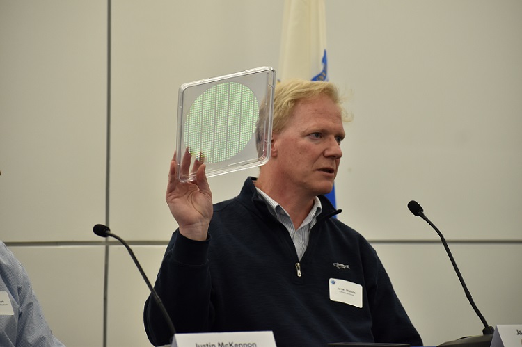
UMass Amherst professor James Watkins holds up a wafer containing a thousand metalenses.
EMA, for its part, will evaluate resulting technologies for durability and viability for its intended purpose. “If we do testing, then we can learn what the limits of a particular design are,” said EMA principal scientist Justin McKennon. “What I think I'm most excited about in this project is learning what knobs that you can turn on a design and what those knobs actually do, because I don't think anybody really knows that about this process.”
Asked about what Berkshire Community College specifically can do to help prepare the workforce, McKennon emphasized the importance of encouraging students to get their "hands dirty," in addition to their classroom education in disciplines such as mathematics.
The UMass-located facility will be open to businesses, such as Watkins’ own Myrias Optics, as well as academia. Along with benefits for the startup and research communities, the facility is expected to provide opportunities for workforce development.
“An important part of this grant is connecting students, educating people on how to do the manufacturing and get them on the shop floor,” Watkins said.
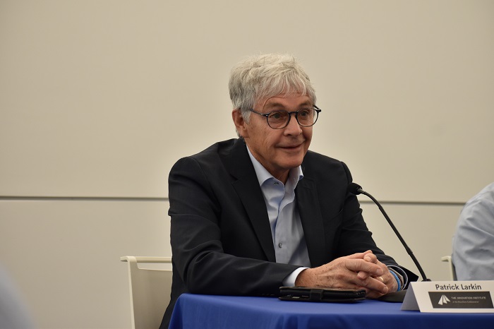
According to Pat Larkin (right), of MassTech, one of the goals of the collaboration is to foster the development of a technology cluster in Massachusetts.