Engineered silicon substrates are providing the foundation for the cutting-edge photonics engines that data centers will need to usher in the era of artificial intelligence.
CORRADO SCIANCALEPORE, TRAVIS HENG, AND LUDOVIC ECARNOT, SOITEC
Courtesy of Chat GPT4, M. Vera Gonçalves, SOITEC.
During the last decade, the exponential growth of data center traffic has been largely fueled by general-purpose cloud- and internet-based applications,
such as video streaming, social networks, internet search engines, and e-commerce platforms. More recently, the onset of artificial intelligence (AI) and machine learning (ML) that leverage large language models (LLMs) for both AI training and inference has added significant upside growth perspectives to the traditional data center market. The transformational effect of this market trend can be easily understood when looking at the evolution of LLMs during the last few years. So far, these models exhibit a super-exponential growth in modeling parameters with a proportionate ingestion of data volumes, as shown in Figure 1 (top). Although it
is still in its early days, the surge in generative AI adoption spans several applications, including robotics, automated
design, advanced augmented/virtual reality, medicine, chemistry, finance, and many others. The combined adoption across all of these markets is propelling the high-performance computing and data center segments into a brand-new techno-economic paradigm.
As Figure 1 (bottom) illustrates, the market share of AI-purposed servers will skyrocket over the next few years, starting from a nearly negligible market footprint in 2022 to reach 50% of overall market revenue — or $90 billion in 2027.
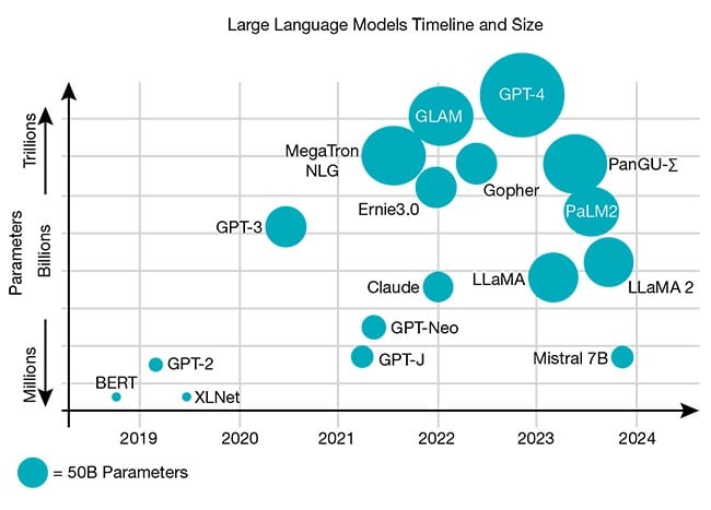
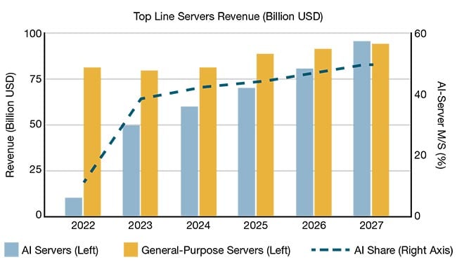
Figure 1. The evolutionary timeline for large language models (LLMs) and relative growth in their number of parameters (top). Top line revenue growth for AI-centric and general-purpose servers, and the relative AI-server market share evolution between 2022 and 2027 (bottom). Courtesy of SOITEC.
Such a rapid rate of growth in inter-data
and especially intra-data center traffic
has driven the need for high-speed optical
pluggable transceivers, which are currently transitioning from 100 Gbps to 400 Gbps. Further, some shipments of 800-Gbps devices already started in 2023 and 1.6-Tbps pluggables are also available today for pre-sampling.
Interconnects and the AI revolution
Pluggable optical transceivers used as data interconnects between servers have an important role to play in the growing demand of AI/ML applications. Inside
a data center, they transmit and receive data between routers and leaf/spine switches. Specifically for cloud AI/ML applications, they interconnect switches and accelerator servers, namely GPU and CPU racks. In addition, these transceivers provide connections between data centers over short, medium, or long distances across metro, long-haul, and subsea networks, respectively.
In general, optical transceivers must address three different, equally important imperatives: high speed, low power consumption, and, ultimately, a minimized cost structure.
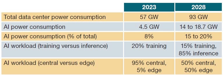
Regarding power consumption, server clusters in a data center deliver power densities between 50 and 100 kW to meet new AI requirements. However, the share of AI workloads, or power consumption in a data center, is expected to more than double between 2023 and 2028 (Table 1).
Table 1. Data Center Power Consumption Trends
Moreover, while a 400-Gbps Ethernet (GbE) pluggable for 500-m to 2-km link distances consumes ~12 W of power, an 800-GbE pluggable typically consumes ~16 W. There is an obvious need for lower-power, higher-speed optical transceivers as data volume grows, which is prompting pluggable form factors to evolve in different architectures. Notably, the digital signal processing (DSP) chip inside pluggable transceivers is one of the main sources of power consumption. This has led the industry to explore novel transceiver designs, such as linear-drive pluggable optics (LPOs), half-retimed linear optics (HALOs), and co-packaged optics (CPOs), to leverage more advanced device design and photonics-electronics co-integration that would enable future pluggables to operate in direct-drive, without a stand-alone, dedicated DSP component.
The key difference between LPOs and traditional optical modules is the linear drive (or direct drive). LPOs apply a
conventional packaging form factor based on a pluggable design that allows for easier transceiver serviceability. As their name implies, LPO transceivers adopt linear, direct-drive technology, eliminating the DSP and clock data recovery
chip from the optical module. As a result, these modules reduce power consumption by ~50% compared with traditional
pluggable optical modules. Further, by eliminating DSPs and using highly linear transimpedance amplifiers and driver chips with equalizer functionality, the LPOs further reduce signal recovery time and latency.
HALOs is a recent, intermediate step between DSP pluggables and LPOs. It
addresses the inherent weaknesses
of DSP-free LPOs. These include interoperability issues, link accountability, and the relative inability to troubleshoot problems.
CPOs have been viewed increasingly as a natural evolutionary step in optical interconnect technology because they can potentially answer the bandwidth and energy efficiency challenges faced by conventional optical pluggables (Figure 2). CPO technology achieves such improvements by directly co-packaging the optical engine chip into the switch or accelerator modules with the application-specific IC (ASIC) or other multi-chip processing modules. This is achieved via advanced packaging processes leveraging the codesign and co-integration of electronics — including advanced digital functions — and photonics. The result is lower latency and lower overall power consumption by directly driving the optical engine via the ASIC or an alternate processing unit, such as a CPU, GPU, and/or memory chip.
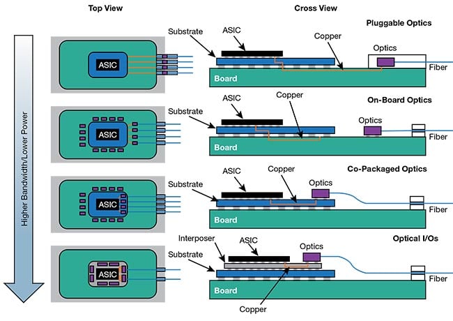
Figure 2. The architectural evolution of optical interconnects from pluggable form factors to more advanced on-board optics, co-packaged optics (CPOs), and optical I/O engines. Optical I/O engines are the ultimate step toward co-integration of digital electronics and photonics. Courtesy of SOITEC.
Enabling cloud AI
In AI server pods and super-pods, GPUs are connected to a networking port that allows them to communicate with GPUs in other racks and accelerator servers. To maximize the efficiency of GPUs’ use, network speed must keep up with the GPU processing and memory storage speeds. This is extremely important for AI applications, where large data sets often need to be processed and analyzed in real time.
To satisfy this demand for the short- to extended-reach connections between GPUs or xPUs (i.e., other GPUs, CPUs, or memory chips), silicon-photonic CPO engines are increasingly considered the key technology for the job. They allow for a more agile system network design between the computing units and local memory, and across the overall AI fabric, thereby providing a three-way improvement of the transceiver function versus legacy pluggables — in terms of cost, performance, and power consumption. Multiple AI companies envision the use of integrated silicon photonics as the next natural evolutionary step for optical interconnects architecture targeting next-generation AI cloud computing infrastructure.
Underlying this evolution are advanced materials platforms on which integrated photonics solutions will be designed and fabricated. The most mature platform is silicon-on-insulator (SOI), which offers
inherent physical and mechanical properties that can benefit multiple silicon photonics applications, especially in the optical networking space (Figure 3).
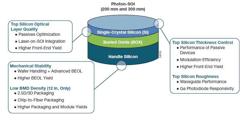
Figure 3. Photonic silicon-on-insulator (SOI) substrates architecture (center) and the technology’s corresponding value proposition for silicon photonic devices, circuits, and subsystems. BEOL: back-end of the line; BMD: bulk micro defects. Courtesy of SOITEC.
Critical to these benefits is enhanced wafer-to-wafer (W2W) and within-wafer (WiW) uniformities and surface roughness of the top silicon device layer of SOI substrates. Additionally, the overall optical properties of the bulk top silicon layer — such as defects, surface states, and bulk microdefects (BMDs) as optical scattering centers — are also important
to provide optimal yield and performance of silicon photonics components. This also ensures as-fabricated devices and circuits are as close as possible to the
as-designed nominals in their computer-aided design (CAD) tool and graphic data stream (GDS) files.
Optical loss is a key benchmark for
assessing the quality of substrate materials because it foretells the overall performance levels of passive devices and subsequent front-end optical yields. This quality is increasingly relevant to large-area circuits as component densities and overall circuit complexity grows with the emergence of advanced, ultrahigh-speed transceivers, on-board optics, and, notably, CPOs.
SOI wafers for silicon photonics are available in both 200- and 300-mm diameters. Larger-diameter substrates can accommodate fabrication of more chips while enabling tighter control over WiW and W2W nonuniformities in top silicon-film thickness. As Figure 4 shows, for SOITEC’s 200-mm-diameter wafers, the current state-of-the-art for top silicon layer thickness WiW range nonuniformity has been reduced by >70% compared to previous generations. Moreover, W2W variability of the average thickness of the top silicon film has also been greatly improved, providing enhanced passive optical performance at wafer scale as well as higher front-end yields when ramping up volume production.
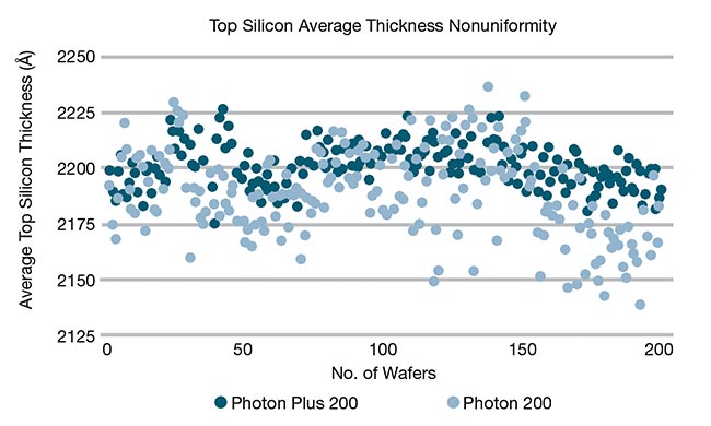
Figure 4. A top silicon average thickness nonuniformity measured over two generations of SOITEC’s 200-mm silicon-on-insulator (SOI) wafers (Photon 200 and Photon Plus 200). The study captured 17 measurement points per wafer for more than 200 wafers. Thickness measurement in Angstroms (1/10 of a nanometer). Courtesy of SOITEC.
This trend was corroborated by optical tests carried out by CEA-Leti on its 200-mm silicon photonics process design kit and test lines. Figure 5 shows optical propagation loss (in dB/cm) of single-mode transverse-electric (TE)-polarized waveguides in both the C- and O-bands for strip and rib configurations. The study from which the data was taken indicates that state-of-the-art SOI technology achieves very advanced targets in terms of top silicon layer film nonuniformity and defect density. This allows current 200-mm SOI wafers to deliver significantly reduced loss (1 to 1.4 dB/cm for strip waveguides), as well as lower dispersion of the median propagation loss value over a wafer (down to 0.09 dB/cm), as indicated by the sigma dispersion in Figure 5 (bottom left corner). Optical loss benchmark tests are summarized in Table 2.
Table 2.
Optical Performance of SOITEC’s Photon/Photon Plus 200
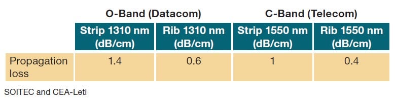
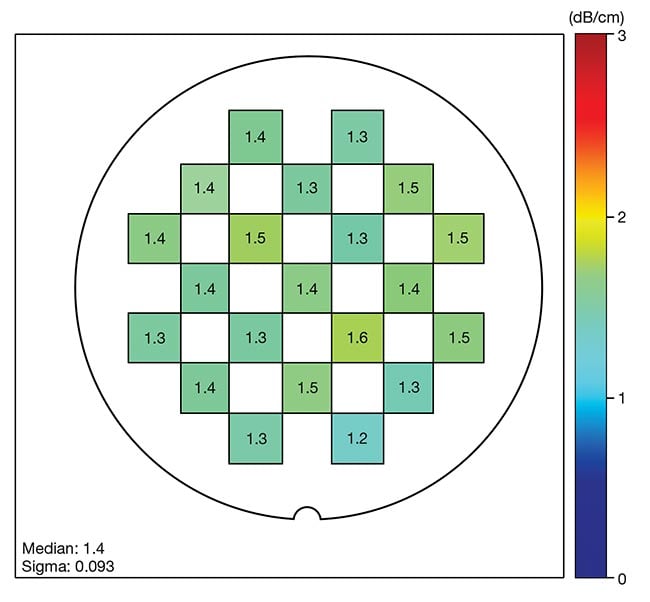
Figure 5. A benchmark of propagation losses (in dB/cm) of single-mode waveguides in strip, transverse-electric (TE) polarized configuration in the 1310-nm wavelength region (left). Courtesy of SOITEC.
Similar benchmark tests that were
applied to 300-mm SOI substrates evaluated devices fabricated at one of SOITEC’s commercial foundry partners. During the tests, the most advanced
SOI wafers exhibited single-mode
TE-polarized waveguide losses ranging
between 0.5 and 0.65 dB/cm WiW and W2W in the O-band. Additional information about 300-mm photonic SOI technology can be found in our previous Photonics Spectra article1.
Advanced packaging for silicon photonics
Advanced packaging and back-end of
the line (BEOL) technologies are the key enablers driving developments on the silicon photonics roadmap, especially
for more advanced transceiver designs and CPO multi-chip module integration. For example, 2.5D and 3D chip-on-wafer-on-substrate (CoWoS) packaging or heterogeneous integration approaches are necessary to provide electrical power supply to increasingly dense and complex silicon photonics chiplets as well as
fiber-to-chip optical connectivity.
Nevertheless, advanced BEOL and module packaging are currently the main yield detractors in silicon photonics.
SOI substrates will have another big role in addressing these challenges. In fact, when looking at the handle of an
SOI wafer, its potential goes beyond merely supporting the trilayer stack.
Advanced SOI processing techniques
that yield superior material chemical-physical properties are providing new
SOI wafers with the mechanical robustness needed to withstand aggressive thermal annealing cycles and thicker, multilayer metal BEOL techniques typical of advanced silicon photonics processing
at foundries. In addition, the handle
silicon should enable foundries and designers alike with sufficient flexibility to implement through-silicon vias (TSVs) technologies and fiber-attach V-grooves (or similar implementations) to provide optical engines with both electrical and optical interconnectivities.
Specifically, interstitial oxygen contained in silicon tends to precipitate on nuclei during SOI fabrication due to thermal treatments, which can lead to
the generation of BMDs. These defects helpfully act as so-called gettering centers that attract potential metallic contamination. They are also needed to ensure that the substrate possesses a mechanical robustness to thermal stress by blocking
the propagation of dislocations, and
hence preventing generation of film-crack defects, generally known as slip lines.
However, the dry etching used to create V-grooves or TSVs in the silicon base substrate are also adversely affected by BMD density. BMDs can cause micromasking during etching and metal-filling processes, leading to defects that can potentially cause major yield losses at foundries due to variability in TSV
resistivity across a die.
To enable new silicon photonics technologies, certain specific developments have helped provide the handle substrate of SOI wafers with the properties needed to address these challenges. Creating a BMD-free zone below the buried oxide of the SOI — also known as denuded zone — yields the double advantage of enabling defect-free etching to form
fiber-attach V-grooves or electrical TSVs while keeping the SOI substrate robust to thermal treatments. This is due to the ability to enable a strong BMD density located below the BMD-free region, as
illustrated by the laser scattering tomography image in Figure 6.
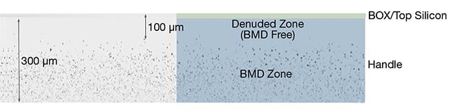
Figure 6. A cross-sectional laser scattering tomography image of denuded-zone handle silicon wafer technology. Bulk micro defects (BMDs) are removed from the denuded zone, measuring ~100 µm in thickness, while BMDs are still present in the lower region to maintain the wafer’s mechanical properties, proper geometry, and overall robustness to thermal, back-end of the line (BEOL), and packaging processing. Courtesy of SOITEC.
AI present and future
With the potential to revolutionize AI algorithms and further advance the capabilities of these complex systems, silicon photonic optical interconnects for AI architectures promise to enable the onset of more efficient fabrics that can accommodate the growingly complex workloads with improved performance. With the inherent evolution of AI networks, silicon photonics alongside heterogeneous integration in multi-chip modules will transform the switching layer, enabling reduced latency and lower power consumption at the interconnect density and cost needed.
Meet the authors
Corrado Sciancalepore, Ph.D., is technical marketing manager and resident senior expert in silicon photonics within the Specialty-SOI Business Unit at SOITEC. He is the author
of more than 125 journal articles and
international conference proceedings on cutting-edge silicon photonics circuits,
III-V optoelectronics, and VCSEL photonics; email: [email protected].
Travis Heng is senior marketing manager
at SOITEC, Smart Devices Division. His responsibilities include identifying market trends and navigating business opportunities
based on the market needs; email: [email protected].
Ludovic Ecarnot is technology manager within the Innovation Group at SOITEC, where he is responsible for the development of silicon photonics technologies; email: [email protected].
Acknowledgment
In frame of the Important Project of Common European Interest for Micro Electronics and Communication Technologies (IPCEI ME/CT). This work benefits from French financial support.
References
1. C. Cailler et al. (2021). SOI Technology Lights Up the Next Wave of Photonics Solutions. Photonics Spectra, Vol. 55,
No. 2, pp. 42-46.