Dr. Sascha Weiler, Trumpf Inc.
When applying picosecond and femtosecond lasers for industrial applications, there isn’t just one ultrafast laser for all applications. Manufacturers need an ultrafast laser portfolio with different powers, pulse energies, wavelengths and price points to fit each specific application.
Fiber laser technology creates an ideal platform for ultrashort pulsed lasers, with low average power and peak powers of 0.5 MW. Combining this ultrafast fiber laser technology with disk laser technology creates another unique platform for high average power and peak powers of several hundred megawatts.
Pico- and femtosecond pulses are short enough torapidly vaporize material without heat transfer to the surrounding material. This makes these lasers game changers in various industrial applications, including cutting of display glass and sapphire, drilling of injection nozzles or cutting of cardiovascular stents.
Solid-state lasers for industry
Since the 1970s, rod-type lasers – first lamp-pumped and later diode-pumped – have been used for industrial production. While pushing the beam-quality limits of high-average-power rod-type lasers in the 1990s, diode-pumped disk laser technology was developed. This became the most reliable and cost-effective technology for kilowatt CW operation for industrial use.
Today, both fiber and disk laser technologies are superior to conventional rod-type lasers. Using a larger cooling surface compared with the laser-active volume enables TEM00 CW operation at power levels up to 4000 W. At equal brilliance, however, the small fiber core inside a fiber laser causes the intensity to be dramatically higher than that of a disk laser. When amplifying pico- and femtosecond pulses, these high intensities lead to nonlinear effects such as self-phase-modulation or Raman scattering, requiring sophisticated chirped-pulse-amplification in ultrafast fiber amplifiers, or limiting the maximum achievable pulse energy to values of 10 µJ or less. Using disk laser technology as the amplifier for picosecond pulses enables high peak power (up to 100 MW at greater than 200 µJ) with low intensities and, therefore, no nonlinearities.
Applying ultrafast lasers
Before using picosecond and femtosecond lasers for industrial applications, it helps to understand how they interact with the material to be processed. Important questions include: How short is short enough for precision machining? And what happens when a laser pulse hits the material, and on which time scales?
The absorption of a laser pulse in metals, for example, is basically an energy transfer from the laser pulse to the electrons of the material. For nanosecond pulse durations, temperature equalization between electrons and lattice sets in. This heat eventually melts the material and partially evaporates it. The shorter the pulses, the faster the energy transfer to the electrons. Ideally, the pulses are so short that there is not enough time for temperature equalization of electrons and lattice. Then, the “hot electrons” (in contrast to the cold lattice) have two ways to couple with the lattice. First, after a specific amount of time, heat diffusion from the electrons to the surrounding lattice begins. This electron-phonon-relaxation time is a material property and is typically between 1 and 10 ps. On approximately the same time scale, but a bit delayed, an abrupt energy transfer between the hot electrons and the lattice takes place, resulting in a phase explosion – i.e., evaporation of the excited volume. Cold processing must therefore be defined as processing with minimum heat diffusion, which requires pulse durations of 1 to 10 ps or less.
Although pico- or femtosecond pulse duration is a necessity for cold processing, additional considerations are required. If the hot electrons become overheated by applying energy density that is too high, heat diffusion effects become visible, and the process becomes thermal. For ablation of metals with pico- and femtosecond pulses without measurable heat effect (i.e., low thermal-penetration depth), energy densities are typically around 1 to 5 J/cm2. However, semiconductors and dielectrics without free electrons allow higher energy densities before heat-diffusion effects occur. When processing glass, for example, higher pulse energy can be translated into more efficient ablation.
A common misconception exists regarding the influence of the linear absorption of pico- and femtosecond pulses. The assumption is that pulses’ peak powers are so high that nonlinear absorption through multiphoton processes becomes dominant to linear absorption. If the described boundary conditions for pulse duration and energy density are met, then this statement is often misleading. Therefore the laser’s wavelength also needs to be considered to achieve proper absorption and high process efficiency.
Furthermore, the laser beam must be manipulated to achieve maximum productivity and quality. Balancing part and feature geometry with accuracy requirements creates many unknown factors. Solving this equation requires a kit of optical components, such as scanners,
f-Theta lenses, focus optics with a coaxial gas nozzle, waveplates, trepanning optics and many others. These must be combined with linear or rotary stages for high precision, or to accommodate tubular part geometry. Although laser technology may be ready for the development, modern linear stages and scanners do not have the dynamics to apply pulse frequencies of more than 1 MHz.
Drilling fuel injector nozzles
Producing fuel-saving, low-emissive engines is a major challenge for the automotive industry. The key is burning fuel more cleanly, which can be accomplished by optimizing the nozzles for fuel injection. Drilling an injection nozzle hole with a high-power picosecond laser produces very sharp edges without burrs or melt, and low surface roughness inside the hole, leading to optimum spray of the fuel. Combining 50-W average power with a pulse energy as high as 250 µJ enables drilling of these high-quality holes with unmatched throughput. It recently became public that this technology, which has been applied by Bosch, reduces a car’s fuel consumption by 20 percent, the company reports.
Cutting display glass
Display manufacturers need to cut glass, but they also must ensure that the cut edge will be of high strength. In addition, industry trends show increased use of ultrathin glass for OLED displays and chemically hardened cover glass, as well as increased demand for flexible shapes and aesthetically appealing designs. Because glass is a brittle yet rigid material, the most common way to cut glass was by mechanically scribing the edge so it could be broken along that line. The resulting edges would typically exhibit cracks, chipping and poor edge strength, which made grinding an unavoidable postprocessing step. Grinding not only limits the flexibility in lateral geometry, but also glass thickness.
Many wide-bandgap dielectrics such as glass are transparent to light in the visible and near-IR spectral ranges; however, the high intensity of picosecond pulses can produce free electrons by means of multiphoton ionization. Because of avalanche ionization, further charge carriers are released, which breaks chemical bonds, thereby ablating the material. One challenge of processing brittle materials is the occurrence of microcracks, which decrease the edge strength. If heat input is too great during processing, material tensions appear and cracks are formed. However, suitable processing strategies may help to avoid the formation of microcracks.
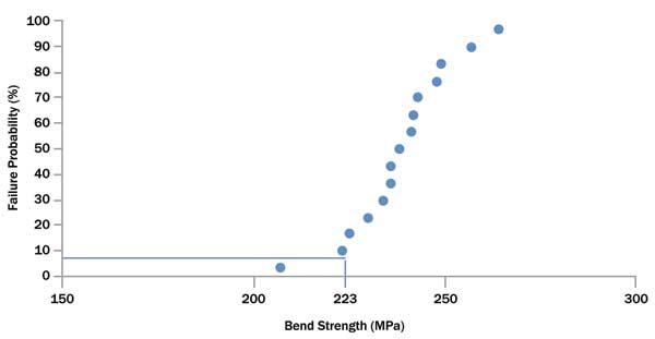
A common method for measuring the flexural strength of a component is the four-point bending test (DIN EN 843-5). Although the occurrence of microcracks and their effect on breaking stress will vary from component to component, they can be described using Weibull statistics. Typically, 10 to 15 samples are processed and applied to the four-point bending test. Figure 1 shows the Weibull distribution of Corning Eagle XG cellphone display glass, which was cut using a Trumpf high-power and high-pulse-energy picosecond laser with a green wavelength, resulting in bend strengths of up to 280 MPa.

Figure 1. The Weibull distribution of Corning Eagle XG cellphone display glass, cut using a Trumpf high-power and high-pulse-energy picosecond laser at a green wavelength, resulting in bend strengths of up to 280 MPa.
Years of application development have led to a breakthrough for picosecond lasers in mass production of mobile displays. Not only in terms of edge quality, but also for flexible (nonlinear) geometries, picosecond lasers have proved to be versatile tools with the ability to cut anything from ultrathin to hardened glass.
Cutting sapphire
Sapphire, the second hardest material on Earth after diamond, is very difficult to process. Cutting sapphire with lasers is a standard process today in LED manufacturing, where sapphire is used as a substrate. Because of its scratch resistance and optical transparency, sapphire is used, for example, to produce covers for wristwatches and protective windows for optical instruments.
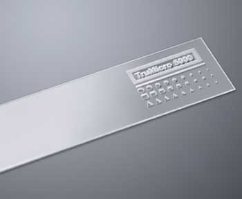
High-power and high-pulse-energy picosecond lasers come into play for processing small contours, for example, when cutting small disks or drilling small holes. Flexible contours can be processed with a galvanometer scanner. The picosecond pulses remove heat effect from the equation, resulting in excellent edge quality. Figure 2 shows 0.4-mm-thick circular, square and triangular contours cut out of sapphire using a 100-W TruMicro 5070 IR picosecond laser. Achieving this excellent quality is a result of optimizing laser parameters, processing strategy, fume exhaust and parts fixture.

Figure 2. A sampling of 0.4-mm-thick circular, square and triangular contours cut into sapphire using a 100-W TruMicro 5070 IR picosecond laser.
Ceramics ablation
Ceramics are high-performance materials. Favorable electrical insulation properties and high temperature resistance make ceramics, such as aluminum nitride, aluminum oxide, silicon nitride and zirconium oxide, popular materials for a wide variety of applications.
Ceramics are an integral part of modern mobile phone antennas, high-performance LED packages and thermal barrier coatings in high-performance jet engines. For most ceramics, including zirconium oxide, ablation rates of 30 mm3/min can be achieved by using a 100-W IR picosecond laser.
Cutting cardiovascular stents
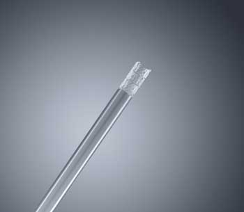
Stent manufacturers attempt to take advantage of polymeric materials, such as those that are bioresorbable. State-of-the-art laser fusion cutting with CW fiber or solid-state lasers can be applied only to metal stents. These lasers also produce melt and burr, which require expensive postprocessing and reduce the yield. With the proper wavelength selection, cutting optics and rotary stage, picosecond lasers can compete with the speed of fusion cutting and provide a distinct advantage in cut quality. This keeps postprocessing to a minimum and results in higher yield. In addition, the same picosecond laser can be used to cut polymer and other nonmetallic stents with high speed and quality, making it a potentially disruptive technology and a universal tool for medical device manufacturing (Figure 3).

Figure 3. A picosecond laser can be used to cut polymer and other nonmetallic stents with high speed and quality, making it a universal tool for medical device manufacturing.
Thin-film ablation
Insulators coated with thin films tens to hundreds of nanometers thick are used in a variety of industries. In the photovoltaic and flat-panel-display industries, touch screens serve as an example of how transparent conductive oxides are often used to create an electrical conductive circuit on glass with high transmission for visible light. In the semiconductor industry, low-k dielectric coatings lower the capacitive losses of a computer chip and allow for higher performance. Coatings such as these must be partially removed to form the pattern of an electrical circuit, separate computer chips or create a functioning multilayer device during the production process.
When processing thin films, the material’s naturally low tolerance of heat input and tendency toward delamination typically leads to masking and etching production processes with limitations in throughput, flexibility and environmental concerns. By using a cost-effective 10-W picosecond fiber laser platform, it is possible to selectively ablate thin films with minimal heat input and, therefore, no delamination from their substrate. In contrast to marking and etching, the pattern generated with a picosecond laser is chemical-free and flexible from part to part or batch to batch.
Meet the author
Dr. Sascha Weiler is the program manager for microprocessing at Trumpf Inc. in Farmington, Conn.; email: [email protected].