Improving the efficiency of thin-film solar cells is a key challenge, and some believe that nanophotonics could be the answer.
Nanophotonic structures give us better control over light, enabling us to manipulate it in ways never seen before – and enabling a new field in optics to emerge, one that marries nanophotonics with energy-saving efforts.
One of the exciting aspects of nanophotonics is its potential to overcome some of the conventional performance limits of thin-film solar cells. Nanophotonics can enhance light-trapping efficiency, which in turn increases the cells’ overall efficiency and reduces the amount of material required, thereby cutting costs.
In a normal photovoltaic approach, incident photons are converted to electron-hole pairs in a semiconductor. The charged particles then drift to an electrode under the influence of an electric field before they can recombine. They are then recovered in an outside circuit as current.
The efficiency of a solar cell can be defined as the ratio of the incident photon flux divided by the number of electrons per second circulating in the outside circuit. A large drop in the efficiency of a solar cell is related to the generation of heat by short-wavelength photons, the energy of which is much larger than the semiconductor bandgap energy. The extra energy beyond the bandgap energy is generating heat in the semiconductor.

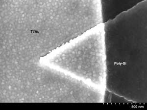
Researchers at the University of Maryland want to use nanophotonics to exploit the electromagnetic radiation absorbed by the Earth during the day and then re-emitted at night. They have demonstrated a nanoantenna coupled to a tunneling diode, pictured here, that uses excited localized surface plasmons. Courtesy of Mario Dagenais, University of Maryland.
“Multijunction solar cells alleviate this problem but are not typically used in low-cost applications because they involve esoteric semiconductors that are costly to produce,” said Mario Dagenais, a professor at the Maryland Nanocenter at the University of Maryland in College Park. “Multijunction solar cells have demonstrated efficiency above 40 percent and are used in specialized applications where efficiency is a dominant requirement, such as in satellite applications.”
About 90 percent of the solar cell market is using single-junction bulk mono- and multicrystalline silicon. “The second-generation solar cells will be based on thin-film solar cells and will use materials such as polycrystalline silicon, amorphous silicon, CIGS [copper indium gallium selenide, or CuInGaSe2], CdTe [cadmium telluride] and other semiconductors.” “The use of nanophotonic structures will be really crucial in both enhancing the efficiency and in reducing the cost of solar energy conversion,” said Shanhui Fan, associate professor at the Stanford Photonics Research Center at Stanford University in California. “It is likely that most advanced solar cell architecture will employ some of these nanophotonic structures in the near future.”

Nanoscale light confinement can boost the sunlight absorption beyond the conventional light-trapping limit. Courtesy of Stanford University.
In a nanophotonic structure, the feature size is comparable to, or even smaller than, the wavelength of light. At or below such a scale, many properties of light-matter interactions are drastically modified. Moreover, in nanophotonics, the properties of a given device are greatly influenced by the geometry, and not by the material alone. As a result, there is an enormous degree of freedom in tailoring novel structures for energy applications.
With nanophotonic structures, the theoretical limit of light trapping efficiency can be an order of magnitude higher than conventional optics would allow, according to Dr. Zongfu Yu and Aaswath Raman, members of Fan’s Stanford group.
“We showed that a nanostructured layer of organic material can absorb over 100 times more light than the same amount of material does without nanostructures,” Yu said. “This is one order of magnitude higher than conventional theory predicts. This effect is achieved by confining the light field into a tiny region of 10 nm.”
Plasmons spread to solar cells
At the nanoscale, the curious world of plasmonics opens up. Plasmons are the collective oscillations of a free-electron gas (plasma), usually found on the surface of metals.
When photons of light are incident upon the surface of the metal, they couple with plasmons to form a plasma polariton or surface plasmon, which can propagate along the surface until it decays by absorption or radiatively into a photon. Such surface plasmons carry light energy as a package of electron oscillations and can exert huge control over electromagnetic waves at the nanoscale.
“Nanophotonics holds great potential in emerging areas related to energy,” Dagenais said. “For instance, it has been recognized for some time that it is possible to excite surface plasmons on metal surfaces and metal nanostructures and concentrate light into deep-subwavelength volumes.”

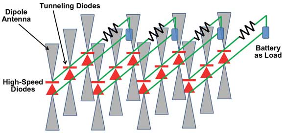
In this solar energy conversion approach, nanostructures can rectify light to generate energy using flexible materials compatible with roll-to-roll technology. A series and parallel combination of rectennas, or rectifying antennas, is shown. Courtesy of Mario Dagenais, University of Maryland.
While the application of nanophotonics and plasmonics to energy-saving efforts is relatively new, a great deal of work has already been published on plasmonic optical antennae for imaging (near-field scanning optical microscopy, for example); plasmon-enhanced detectors with less noise and enhanced speed; spectroscopy applications (surface-enhanced Raman scattering); plasmonic lenses that go beyond the diffraction limit; and plasmonic resonators with small volumes and reasonable field enhancements.
By comparison, few papers have discussed the use of plasmonics in energy applications – but the situation is changing rapidly.
“New microfabrication techniques like proximity-corrected e-beam lithography and nanoimprinting are critical in creating the ultrahigh-resolution and volume manufacturing capabilities needed to make this approach useful,” Dagenais said. “In energy applications, nanophotonics will permit new designs of solar cells with enhanced absorption, leading to thin-film solar cells with enhanced efficiencies, and new solar cell designs using new materials, and new approaches to using surface plasmons, nanoantennas and tunneling diodes to directly rectify the optical radiation.”
Thanks to new plasmonic concepts based on metallic nanoparticles or new antenna structures, light is scattered in new directions. This increases the path for absorption and permits a sizable reduction in the thickness of the solar cell absorber layers.
This will lead to highly efficient thin-film solar cells and may avoid some of the problems of material scarcity for some types of solar cells – for example, CIGS and CdTe.
Metal nanoparticles measuring less than 100 nm in size can be sprinkled on the surface of the solar cell. The electric field of incident electromagnetic radiation excites the free electrons in these metal particles, and the incident light can be scattered or absorbed.
At a particular driving frequency, a resonance is achieved, and the electric field in the near vicinity of the particles is greatly enhanced – by two to three orders of magnitude, depending upon the quality factor of the resonance.
“Nanophotonics allows new ways to couple, concentrate and change the wavelength response of the material to light,” Dagenais said. “Because of the small dimensions involved, it is now possible to design structures with minimal capacitance to directly rectify the light and generate DC power. Using techniques based on molding, nanoimprints and replication, one can imagine producing a large number of nanostructures to rectify the light and generate energy and use flexible materials compatible with roll-to-roll technology.”
Solar cells that work at night
Today’s solar cells work only when there is sufficient sunlight, which limits their use to areas that receive a decent amount of sunlight throughout the year. But imagine a solar energy converter that could work efficiently when it is cloudy or raining, or even at night.
Dagenais and colleagues are working toward achieving this goal. The fundamental idea is to use nanophotonics to exploit the electromagnetic radiation that is absorbed during the day by the Earth, and that is then re-emitted.
“As with any object in thermal equilibrium, Earth absorbs solar energy from the sun during daytime and then continuously re-emits it at night,” Dagenais said. “At thermal equilibrium, the Earth absorbs and re-emits the same amount of energy. The peak wavelength of this reradiation spectrum falls at around 10 µm. So if a device can detect this wavelength and also convert it to electricity, that would be most interesting.”
Of course, Dagenais is not suggesting that the second law of thermodynamics can be broken, but he does believe in the feasibility of scavenging energy from the environment in a situation where the antenna is not in thermal equilibrium with its surroundings.
The researchers are the first to demonstrate a nanoantenna coupled to a tunneling diode that uses excited localized surface plasmons. In the setup, a bow-tie antenna focuses incident radiation to the neck of the bow tie. The electric field in the gap of the antenna is strongly enhanced, and it is in this region that a dielectric layer is positioned, which permits resonant tunneling of the electrons gathering at the apex of the antenna.
“Our optical nanoantenna is therefore directly coupled to a tunneling diode, a rectifying metal-insulator-metal diode,” Dagenais said. “The optical nanoantenna acts as a receiver of the infrared radiation much as a normal [radio-frequency] TV antenna does and then couples this radiation to a rectifying diode to yield a DC output current.”
So far, the team has demonstrated operation of the device at 20 GHz and soon hopes to report infrared detection at 10 µm. One key advantage of the approach is that it does not require a direct bandgap semiconductor and avoids the minority carrier lifetime limitations in solar cells.
Although researchers in the field have been successful in demonstrating concepts, one of the challenges facing those using nanophotonics in energy applications is to optimize successful designs and scale up the technology. The goal is to build a large number of nearly identical nanophotonic devices that span large areas for energy collection.
“A breakthrough would be to demonstrate a cheap thin-film silicon solar cell with material costs much lower than bulk silicon and efficiencies similar to bulk solar cell efficiencies with nanotechnology that can be scaled up at low cost,” Dagenais said.