Michael Watts, Spectra-Physics
Throughout the electronics industry, the demand for more functionality and reduced package size continues unabated. This, in turn, requires integrated circuits and printed circuit boards with higher density, improved performance and more flexible packaging options. One emerging technology supporting this is the use of embedded passive components, electronic components formed within a laminated circuit board.
Modern printed circuit boards comprise a series of panels (usually FR-4 composite) laminated into a multilayer circuit board. The term “embedded passives” refers to resistors and capacitors formed as localized thin films on one or more of these panels.
One company that supplies integrated laser equipment for this application is Electro Scientific Industries Inc. (ESI) in Portland, Ore. “Compared to the use of discrete, surface-mounted components,” said ESI researcher Kim Fjeldsted, “this embedded approach potentially offers several important benefits, including conserving valuable board space, increasing performance, reducing manufacturing cost and improving reliability. It also enables use of more cost-effective substrate materials.”
GSI Lumonics of Ottawa also supports this application. “There is already a broad range of resistor materials that have been developed by companies such as DuPont, Asahi, Gould, McDermid and Ohmega Technologies,” said GSI researcher Paul Chase. “These materials can be loosely categorized as thin-film and thick-film devices. Thick films include several types of ceramic paste, which are then baked. Another thick-film material is epoxy-based polymer loaded with carbon or metal flakes. Resistive thin films are produced on copper foil, which is then etched away. In another process, copper and thin-film resistors are both patterned using photomask and chemical etching techniques.”
Laser trimming
Typical resistance tolerances for embedded devices are ±10 percent or worse. But many consumer applications for these printed circuit boards require tolerances closer to ±1 percent. The most promising way to accurately adjust resistor values is laser trimming, which is already proven and cost-effective for trimming discrete resistors on ceramic substrates in hybrid circuits.
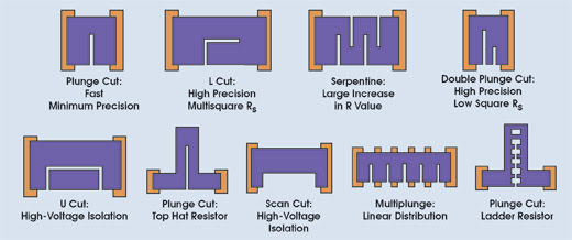
For material with a given film thickness and resistivity, device resistance is inversely proportional to the effective area of the resistor confined between the two contact electrodes. Several types of laser cuts can change this effective area (Figure 1). Two of the most common geometries are plunge and L cuts. A single plunge cut usually represents the lowest cost and is suited for applications where high process speed and low costs are paramount.

Figure 1. A single plunge cut is often the most economical trim option in applications with high processing speed. Courtesy of GSI Lumonics Inc.
To understand the purpose of some other cut geometries, it is important to note that laser trimming involves closed-loop control. A voltage is applied to the resistor, or part of the board, using probe tips. The cutting proceeds until the voltage or current measured by other probe tips reaches a target value. The L cut starts with a cut perpendicular to the current flow, which results in a very rapid increase in the resistance value. Once this value starts to approach the target value, system software redirects the laser cut parallel to the current flow. In this orientation, the resistance changes very slowly with cut length and allows approaching the final value with great accuracy.
Serpentine cuts are used where design and other manufacturing constraints require a final resistor value significantly larger than the resistance as initially deposited or formed. The U-shape cut allows voltage isolation — to avoid shorting across the cut. For even higher voltages, the scan cut allows complete removal of an area of resistor material. It also is useful for avoiding the formation of parallel plates and capacitive reactance components in high-speed applications.
The typical integrated trimming system includes a laser, beam delivery and focusing optics, fast galvanometers for scanning the laser spot, semiautomated or fully robotic equipment for handling and positioning panels, probe electronics and system software. “The goal is to cut the resistor with the highest speed,” Chase said, “while achieving accuracy requirements and avoiding any damage to the FR-4 panel material.”
Laser trimming systems for embedded passives usually incorporate an Nd:YAG laser generating between 5 and 10 W of average power at 1.06 μm. Although many micromachining applications now use Nd:YVO4 lasers, Nd:YAG is preferred here because it delivers relatively high energy per pulse. A typical model used in this application is the Navigator Y70SC-106Q from Spectra-Physics, with pulse repetition rates adjustable up to 100 kHz and pulse energies greater than 1.5 mJ.
Why diode-pumped instead of lamp-pumped lasers? According to Fjeldsted, “These lasers provide the critical requirements of flexibility and pulse-to-pulse stability.” Flexibility refers to the ability to vary pulse energy and repetition rate without compromising the output mode quality. Diode-pumped lasers produce a smooth Gaussian profile with no hot spots, which could otherwise limit accuracy of the trim process and could damage panels.
In practice, bite size (the hole diameter produced by a single laser pulse) and pulse rate determine the maximum trim rate. Typical bite size is 1.5 to 15 μm, depending on the resistor material and its thickness. The overlapped laser pulses must completely cut through the resistor film without damaging the underlying panel. Also, Chase noted that there must be at least a 50 percent overlap between consecutive bites to produce a cut with smooth edges.
Printed circuit board manufacturers measure resistor trimming accuracy using three statistical parameters: χ, 3σ and Cpk. Sigma (σ), the standard deviation of the trimmed final product, is a good measure of the spread of final values but not of any net offset. On the other hand, the process capability index, Cpk, is a statistical ratio of the offset mean value and 3σ. The higher the Cpk value, the better the process.

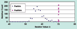
Figure 2. ESI supplies integrated laser systems for trimming applications. Shown are data for 70-Ω polymer thick-film resistors.
At the IPC annual meeting in October 2002, ESI engineers reported statistical data for different resistors that had been trimmed in their applications laboratory. With 1137 resistors per panel, two types of resistors were trimmed to value with final Cpk values greater than 2.0 at 1 percent tolerance and greater than 10 at 5 percent tolerance.
Contact: Michael Watts, product manager, Spectra-Physics, Mountain View, Calif.; +1 (650) 966-5761; fax: +1 (650) 961-9049.