|
Thursday, January 9, 2020 |
|

|
|
|

|
| sponsor |
 |
|
Quantum Sensors in Diamond Anvils Measure Performance Under Extreme Conditions
A team of scientists led by the U.S. Department of Energy’s Lawrence Berkeley National Laboratory (Berkeley Lab) and University of California, Berkeley (UC Berkeley) took advantage of the intrinsic sensing properties found in nitrogen-vacancy (NV) centers — atomic defects found in a diamond’s crystal structure — to develop a tool that can be used to perform experiments that are inaccessible to conventional sensors.
|
|
|
|
|
|
Researchers Build Chip-Size Particle Accelerator
Scientists at Stanford University and the SLAC National Accelerator Laboratory have created a silicon chip that can accelerate electrons using an infrared laser to deliver, at less than a hair’s width, the sort of energy boost that takes microwaves several feet.
|
|
|
|
|
|
Neural Networks Train Lasers to Spot Space Junk
A set of algorithms for laser ranging telescopes, developed by scientists from the Chinese Academy of Surveying and Mapping and the Liaoning Technical University, is improving the success rate of space debris detection in Earth’s orbit by significantly improving the pointing accuracy of the telescope.
|
|
|
|
|
|
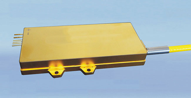
 Wavelength Stabilized Diode Laser
PhotonTec Berlin GmbH
PhotonTec Berlin extends the wavelength stabilized product family with a new diode emitting up to 200 W through a 200 m core, NA 0.22 fiber at 976 nm. Utilizing volume grating, the emitting wavelength is stabilized at 976 nm and insensitive to operating temperature and current.
Visit Website
Request Info
|
|
|
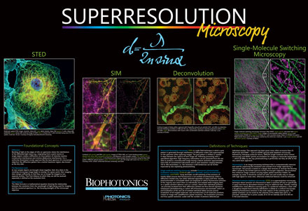
 Superresolution Microscopy Poster
Photonics Media
With interest in the superresolution microscopy field growing rapidly, the editors of BioPhotonics magazine — in collaboration with acknowledged experts — created a poster with readers in mind that is suitable for lab, classroom and office.
Visit Website
Request Info
|
|
|
|
|
|
NUS Singapore Develops Large-Area, Flexible NIR LEDs
A research team led by Tan Zhi Kuang from the Department of Chemistry and the Solar Energy Research Institute of Singapore (SERIS) has developed high-efficiency, near-infrared LEDs that can cover an area of 900 square millimeters using low-cost solution-processing methods.
|
|
|
|
|
|
Researchers Achieve 3D Printed Glass with Complex Geometry
Researchers from ETH Zürich have developed a technique to produce complex glass objects with 3D printing. The method is based on stereolithography, one of the first 3D-printing techniques developed during the 1980s. The process allows objects to be built up layer by layer, with parameters that can be changed on a layer-by-layer basis, including pore size.
|
|
|
|
|
|
DenseLight to Expand in Singapore and China After Ownership Transfer Read Article
Natural and Artificial Vision Combined to Treat Blindness Read Article
Scientists Develop Spectrometer to Detect Molecular Signatures Read Article
Osram, Rinspeed to Debut Modular Electric Vehicle at CES 2020 Read Article
Titan Enterprises Proposes Solution to Cooling World’s Most Sensitive Astronomical Camera Read Article
|
|
|
|
DesignCon 2020
January 28-30, 2020 - Santa Clara Convention Center - Santa Clara, Calif.
North America's largest chip, board, and systems event, DesignCon, returns to Silicon Valley for its 25th year. This three-day event brings together the brightest minds across the high-speed communications and semiconductor industries who are looking to engineer the technology of tomorrow. With more than 100 technical paper sessions, panels, and tutorials spanning 14 tracks, DesignCon’s three-day conference program covers all aspects of hardware design. The latest in high-speed design tools, technologies, and developments will be on display at the DesignCon expo. Offering more than 175 suppliers, DesignCon remains the place for chip, board, and systems design engineers to source, network, and stay ahead of industry change.
|
|
|
|
Advancements in Precision Motion Control for Electro-Optical Manufacturing and Laser Materials Processing
Wed, Jan 22, 2020 1:00 PM - 2:00 PM EST
With a focus on high-throughput/high-yield positioning and microrobotic solutions for leading-edge manufacturing, this webinar from Physik Instrumente (PI) will present the latest advancements in software, control algorithms, and motion systems hardware available to design engineers and scientists in the laser processing, optics, and photonics industries. Examples will include laser processing of substrates with nonuniform topologies and autonomous microrobotic and precision-positioning solutions for fast optimization in the manufacture of silicon photonic, laser electro-optic, lidar, and imaging-optic assembly and test.
|
|
|
|

CALL FOR ARTICLES
Photonics Media is currently seeking technical feature articles on a variety of topics for publication in our magazines (Photonics Spectra, BioPhotonics, Vision Spectra, and EuroPhotonics). Please submit an informal 100-word abstract to editorial@Photonics.com, or use our online submission form.
|
|
|
|
 |
|