 Electro-Optical Wafer Tester
ficonTEC Service GmbH
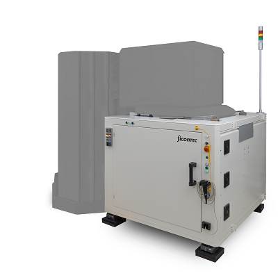
ficonTEC’s 300-mm double-sided electro-optical wafer tester enables high-throughput testing of silicon photonic integrated circuit (PIC) devices at wafer level. Utilizing automatic test equipment architectures, the system’s optical test cell docks with it at a software and hardware level enabling DC and high-data-rate test capability on the top side and precision optical six-axis active alignment probing below.
|
|
 Hexapods in Stock
PI (Physik Instrumente) LP, Motion Control, Air Bearings, Piezo Mechanics
PI hexapods simplify complex 6-axis motion tasks with advanced algorithms and intuitive software. They support any orientation and offer a wide range of load, precision, and travel specs. Applications include photonics alignment, drone testing, optics/panel alignment, and dynamic machining.
|
|
|
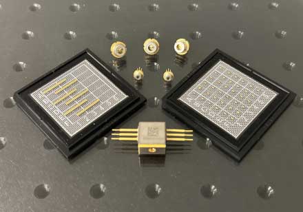 GaN Lasers
Kyocera SLD Laser (KSLD)
KYOCERA SLD Laser, Inc. is the only US-based GaN laser company – fully vertically integrated including wafer growth. We offer laser chips, chip-on-submount, and bars in a variety of wavelengths including 405, 520, and 445nm. Offering multi-Watt multimode chips, high power single mode, frequency narrowed, custom SLEDs and laser-phosphor white light sources.
|
|
 Image Sensor Module
Hamamatsu Corporation
The C16795 series from Hamamatsu Photonics is an image sensor module for imaging applications including real-time nondestructive inspection techniques such as food screening, plastic sorting, semiconductor inspection, and traffic monitoring using hyperspectral imaging.
|
|
|
|
| |
|