|
Thursday, November 5, 2020 |
|
Join us for a FREE Webinar
Applications for Video and High-Resolution Hyperspectral Imaging
Thursday, November 19, 2020 1:00 PM - 2:00 PM EST
|
|
Presented by
|

|
|

|
A hyperspectral camera captures the light that is reflected by an object or transmitted through a material. And since every material has its own specific spectral fingerprint, it can be identified in this object. Thanks to machine learning and other novel algorithms, this can be translated into interesting details such as water content, age, authenticity, and so on.
In the past, hyperspectral cameras were complex and expensive pieces of equipment, mainly for use in the lab, and they required large computers to process the data. Today, there are solutions that transform these complex giants into user-friendly and compact devices. The most integrated and miniaturized solution today is provided by imec’s on-chip spectral-filter technology. In this webinar, details will be given on imec’s hyperspectral imaging technology and the novel applications it enables.
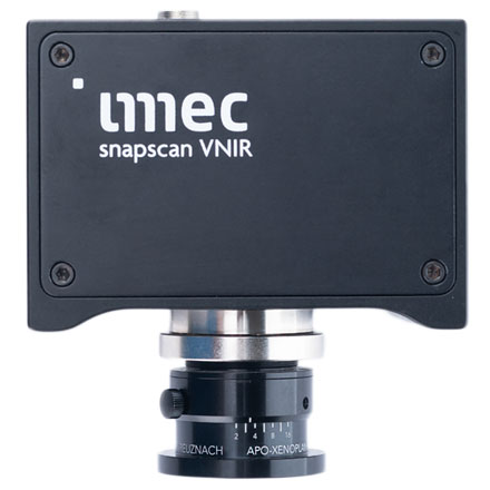
The evolution of cameras incorporating imec’s compact hyperspectral sensors will also be presented. Imec has developed both high-resolution hyperspectral scanning cameras and multispectral video-rate cameras, cameras for labs and microscopy, and cameras for remote sensing and applications outside the lab. The requirements of every customer and application are different. For this reason, imec tailors its collaboration model, ranging from off-the-shelf cameras/software to sensor customization and manufacturing projects tuned to one’s specific needs.
In this webinar you will learn how the unique capabilities of hyperspectral imaging are applied to innovate businesses, applications, and research. Next to some insights on imec’s unique on-chip technology, advanced imaging software and comprehensive support tools, the presenters will give an exclusive look into imec's hyperspectral-imaging demo studio to show some of their off-the-shelf camera systems in real life.
Who should attend:
Anyone designing systems for surveillance, robotics, precision agriculture, remote sensing, quality control, medicine and health, forensics, art and heritage, and more. Those whose applications require more detailed information on material composition or color to make better decisions—for instance, to know when a plant is stressed; to distinguish between different types of plastics or fabrics; to measure blood perfusion and oxygenation; to assess fruit ripeness or the amount of fat content; or any other useful insights that spectral imaging can provide. This presentation is the perfect way to start your hyperspectral journey and to find out exactly what hyperspectral imaging can mean to you.
About the presenters:
Paul Danini is in charge of business development of the imaging activity at imec. After a short experience in IP strategy and management at Avenium Consulting, he carried out market reports and marketing studies on the imaging industry at Yole Development. He joined imec in 2019 after five years as product manager for linescan cameras and CMOS image sensors at Teledyne e2v.
Wouter Charle is manager for hyperspectral imaging technology at imec, leading the off-the-shelf and evaluation system activities. He has a background in physics and software engineering. After starting his career in 3D machine vision, he joined imec in 2014 to help grow the hyperspectral imaging business.
About imec:
Imec aims to be the world-leading R&D and innovation hub in nanoelectronics and digital technologies. As a trusted partner for companies, startups, and academia, imec brings together brilliant minds from around the world in a creative and stimulating environment. By leveraging its world-class infrastructure and local and global ecosystem of diverse partners across a multitude of industries, the company is accelerating progress toward a connected, sustainable future. With a background in semiconductor fabrication, equipment, and process technology, imec designs and manufactures interference-based optical filters at wafer level, deposited and patterned directly on top of image sensor pixels. This unique CMOS-based infrastructure provides very compact, clean, and high-yield optical filter integration with scalability to high volume and low cost.
|
|
|
|
Date: Thursday, November 19, 2020
Time: 1:00 PM - 2:00 PM EST
Space is limited. Reserve your Webinar seat now at: https://attendee.gotowebinar.com/register/4235028929215227662
After registering you will receive a confirmation email containing information about joining the Webinar.
|
|
|
SYSTEM REQUIREMENTS
Operating System
Windows® 7 or later, Mac OS® X 10.9 or later, Linux®, Google ChromeTM OS
AndroidTM OS 5 or later, iOS® 10 or later
Web Browser
Google ChromeTM (most recent 2 versions)
Mozilla Firefox® (most recent 2 versions)
Mobile Devices
AndroidTM 5 or later
iPhone® 4S or later
iPad® 2 or later
Windows Phone® 8+, Windows® 8RT+
|
|
|
|
.: More from Photonics Media
|
|
|
|