Bandpass filters are passive optical devices that control the flow of light. They are used to isolate certain wavelengths or colors. Applications range from detecting the gaseous composition of a distant star to visualizing the chemical activity in a human cell. Ultraviolet (UV) bandpass filters (with effective wavelength ranges below 400 nm) pose unique design and manufacturing challenges related to the absorption of materials at short wavelengths.
Sarah Locknar, PhD, Omega Optical LLC, an Omega Optical Holdings company
In their earliest forms, UV bandpass filters that were optimized for wavelengths less than 400 nm, such as the Schott UG or the Hoya U-series, were constructed of absorbing compounds in glass. Such filters were limited by the available compounds that can be dissolved or suspended in glass, and they typically had a gradual transition from low to high absorption (Figure 1). These properties in turn limited the applications to ones that do not require sharp or user-defined transitions between transmission and blocking. These limitations were overcome with the development of interference filters, which were made by depositing a multilayer optical coating onto one or more transparent substrates, thus producing a more refined transmission band surrounded by regions of low transmission (the blocking region).
Metallic-dielectric-metal (MDM) bandpass filters
Many UV interference bandpass filters employ metallic films. To manufacture them, a metal film with high reflectance and limited absorbance is deposited under vacuum onto a transparent substrate. This is followed by a nonabsorbing dielectric thin film of appropriate thickness and refractive index and then by another metal layer. The resulting stack minimizes the reflection in a specific wavelength range with a corresponding increase in transmission (induced transparency) while other wavelengths remain unaffected and therefore continue to reflect incident energy, which results in the blocking of light over a large wavelength range. In Figure 2, the peak transmission is relatively high but the blocking is only OD2, which is insufficient for most applications. There is a trade-off between transmission and deep blocking in these designs because of absorption by the metal. All the light has to be accounted for in an optical design so that I0 = R + T + A, where I0 represents the incident light intensity, R the light that is reflected (both specular and diffuse), T the light that is transmitted, and A the light that is absorbed. Peak transmission decreases as the absorption and reflection increase because of the thickness of the metal.
Blocking can be increased by condensing metal films onto a substrate where several metal layers are separated by nonabsorbing dielectric materials. This multilayer construction acts as a Fabry-Pérot (FP) interferometer. The industry refers to this FP stack as a cavity. Higher-order harmonics occur at shorter wavelengths and are usually absorbed by the materials as described in the next section.
Dielectric materials for UV interference filters
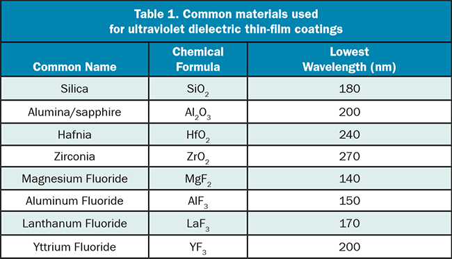
In order for an induced transparency design to be effective, the second (or dielectric) material must be nonabsorbing to keep the transmission as high as possible. Besides the coating materials themselves, another factor to consider when designing UV filters is the substrate. Many materials, including commonly used oxides and sulfides, begin absorbing below 350 nm. Fluorides transmit the lowest wavelengths and can be used for designs below 200 nm (Table 1). Sometimes the absorption of a material can be beneficial when used as the low-wavelength edge of the filter design.
Traditional materials used in interference filters maximize the refractive index mismatch between high-index materials and low-index materials. Maximizing this difference permits the reduction of the total number of layers in the design and ultimately of the thickness of the film stack. The thin layers of material are deposited onto the substrates using a variety of methods, including physical vapor deposition, e-beam with or without ion-assist, and sputtering methods (magnetron sputtering, plasma-assisted reactive magnetron sputtering, ion beam sputtering, etc.). The process method and the number of layers and their thicknesses are strong cost-drivers for interference filters.
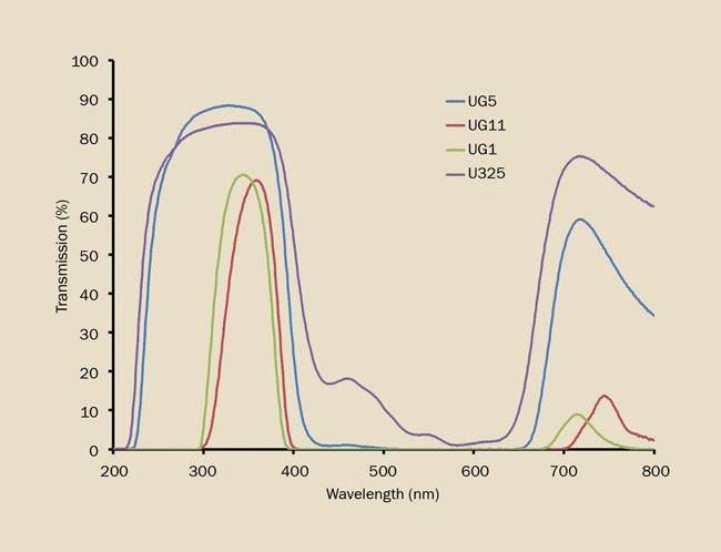
Figure 1. UV transmitting glasses are designed to transmit some UV wavelengths while absorbing the bulk of the light in the visible wavelengths.
All-dielectric UV bandpass filters
Historically, filter manufacturers designed bandpasses based on the model of an FP interferometer, allowing for optical monitoring of film growth based on λ/4 increments that are easily visible to the thin-film technician. The FP principle states that reflection will be canceled when a standing wave exists between two reflectors. The technician creates reflectors using stacks of alternating high- and low-index dielectric layers. These reflectors are optimized for the bandpass of interest and are separated by a spacer layer to set up the standing wave of a single FP cavity. The primary feature of this type of bandpass is that peak efficiency is very high with 100% transmittance if materials with zero absorbance are used. The bandwidth of a single-cavity FP filter is determined by the degree of reflection within the FP interferometer. With reflection of 95%, the bandpass will be on the order of 1 nm full-width at half max (FWHM) (Figure 2). At the center of the band, the transmission will exceed 90%, while the attenuation outside of the bandpass is relatively narrow with a maximum attenuation of OD3. A wider bandpass can be achieved by reducing the reflectivity. With reflectors of 90%, the bandwidth would be 10 nm, but the attenuation would only be OD2. This level of attenuation is not adequate for most filter applications.
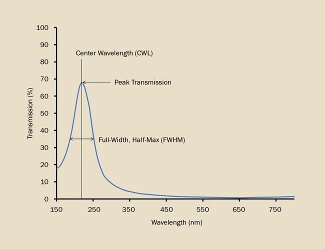
Figure 2. An induced-transparency filter with three layers in an MDM arrangement.
Increasing the number of cavities has a number of uses in the design process. A wide bandpass can be generated by increasing the number of cavities while reducing the number of layers per cavity (or reflectivity within the FP, as described earlier). Increasing the number of cavities brings the OD back up to the desired level while preserving the wide bandpass. As the number of cavities is increased, the shape of the transmission band becomes more rectangular (Figure 3). Keeping a large number of layers in each cavity while adding cavities permits the design of a filter with very steep edges.
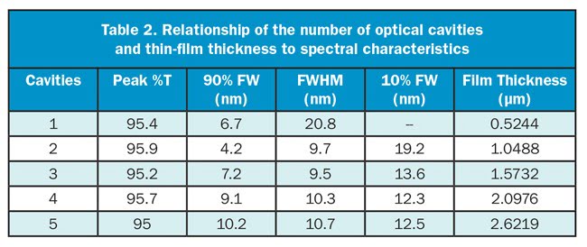
The traditional FP bandpass filter made with nonabsorbing dielectric interference only provides effective blocking around the region of the defined transmission band ±~20% (Figure 3b). Outside this region, the thin-film layers deviate from a phase thickness where controlled interference occurs, resulting in rapid oscillation from reflection to transmission. Increasing the number of cavities increases the blocking depth and slightly decreases the blocking wavelength range (Figure 3b). As the number of cavities increases, the peak transmission stays relatively constant while the edge steepness increases significantly (Figure 3a). Table 2 shows a comparison of full-width at 90%T and at 10%T. As the designs increase in the number of layers and complexity, the ratios of full-width at 90% versus 10% become closer and closer to one. The thickness of the film stack also increases, which increases production time and cost.
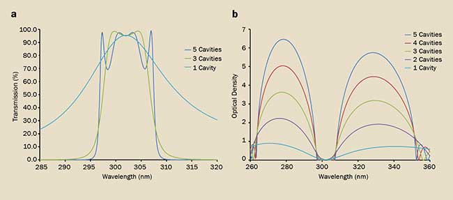
Figure 3. Dielectric filters with an increasing number of cavities in the simple FP design. Peak %T is not significantly affected by an increase in the number of cavities (a), but blocking and edge steepness of the bandpass increases with the number of cavities (b).
Blocking strategies in UV filters
As discussed earlier, the absorption of UV light by most materials makes it difficult to achieve short wavelength bandpasses and high %T with deep blocking over a wide wavelength range. This is particularly true for bandpass filters in the UV. Customers should carefully consider their blocking requirements at longer wavelengths, because blocking the entire visible range and into the NIR is extremely difficult and should only be requested when absolutely necessary. Nearly all blocking strategies substantially increase cost and reduce performance in the passband.
For instance, in the case of creating a filter for a portion of a mercury gas lamp, broadband blocking is not generally required because the source exhibits discrete emission lines. Shown in Figure 4, is an example of a filter designed to pass the 253.7 line of Hg, while blocking the other lines. There is very little light from the lamp around 500 nm, so the blocking can be neglected in this region, reducing the complexity and cost of the filter.
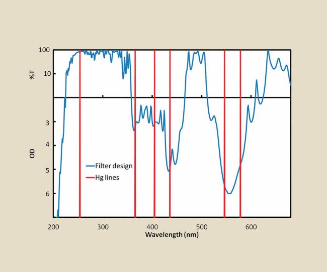
Figure 4. A dielectric filter designed to transmit the Hg line at 253.7 nm while blocking other spectral lines.
As shown in the models in Figure 5, a bandpass filter at 300 nm can be blocked using various methods. Note that this is a log scale. The bandpass filter alone is composed of a dielectric stack that is ~4.5 µm thick and provides blocking in a relatively narrow wavelength range. If this filter is deposited on UG5 glass that is 3 mm thick, the spectrum is shown in green and shows moderate (OD2) blocking over the visible range with some deeper blocking in spots. For full blocking, an additional dielectric stack (8.3 µm thick) is added to the other side of the UG5, resulting in the purple curve. Another option is to use a thicker dielectric blocker on the second side of a fused silica substrate (red curve). To provide blocking over such a wide wavelength range, this stack must be >11.5 µm thick. Advantages of dielectric blockers include reduced effect on %T (Figure 5b) and greater control over the total thickness of the part. The addition of colored glass typically increases the total filter thickness. Long-range blocking options for bandpass filters at wavelengths <250 nm are limited to primarily MDM coatings.
The refractive index difference of dielectric materials used for UV coatings decreases as the wavelength moves into the visible and NIR wavelengths. As the refractive index difference decreases, the number of layers must increase to achieve the desired results. Filters often require several hundred layers to achieve the desired spectral control into longer wavelengths. Theoretical attenuation of >OD20 can be achieved, and measured values of OD10 have been demonstrated. Another practical issue to consider in thick dielectric coatings (not included in the models in Figure 5) is diffuse scattering of the incident beam. Thin films often contain nano/microcrystalline domains that show increased scatter as the wavelength decreases and the thickness of the film increases, especially in sputtered films.
In practice, pinholes in thin films can wreak havoc on OD specifications. Even a small pinhole or defect can induce a measurable change in the OD. Small pinholes do not necessarily affect the performance of the system if the filter is positioned outside of a conjugate or imaging plane.
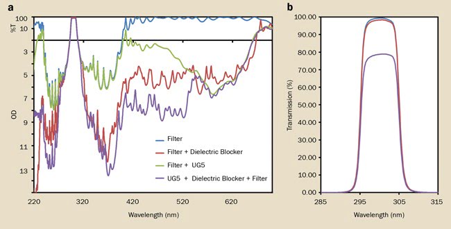
Figure 5. Different blocking strategies for a 300-nm dielectric bandpass filter (a) and the effect on %T (b).
Consider geometry in optical designs
As described above, most materials used for thin-film coating start absorbing light in the UV. This makes it very difficult to produce a highly transmitting UV filter while simultaneously blocking the full visible spectrum. Switching to a reflecting, or baffle box, configuration allows for high %T in the bandpass and good blocking in the visible thanks to the use of absorbing epoxies or anodization in the assembly (Figure 6). The design for this filter is a rejection band that attenuates 280-nm light in transmission. When used in a reflective configuration with a light-absorbing mount, it acts as a bandpass filter. The blocking can be increased by increasing the number of bounces in the system. Keeping the angle of incidence low (<~25°)
minimizes polarization effects. This strategy can be used in many optical designs, enabling a clever designer to integrate beam steering and wavelength control functions into a single optical component.

Figure 6. A multi-bounce reflected filter assembly at 22.5° angle of incidence.
The future of UV filters
With modern, computer-controlled deposition systems and design software, thin-film designers are no longer limited to FP designs. Small tweaks to
the thickness parameters enable high %T in the entire bandpass with much lower ripple than that shown in Figure 3b while maintaining very high blocking. It is also possible to design filters that encompass the bandpass and blocking in a single stack that can be deposited onto a single side of the substrate. These designs have problems of their own, including increased optical scatter and stress-induced deformation of the substrate.
As additional applications for deep-UV are developed, filter technology will undoubtedly follow. Research into new materials and processes and ways to minimize scattering and pinholes is ongoing and will continue.