Full company details
MKS/Newport
 8 East Forge Pkwy.
Franklin, MA 02038
United States
Phone: +1 508-528-4411
Fax: +1 508-520-7583
Toll-free: +1 800-598-6783
Positioning Technology Proves to Be Pivotal in High-Precision Manufacturing
Photonics Spectra
Jan 2025The drive for miniaturization continues. Nanopositioning technology is advancing to meet the needs of component and device fabricators worldwide.KNUT HAUKE AND MARC SCHENKELBERGER, MKS NEWPORT
As it relates to semiconductor and electronics manufacturing, miniaturization seems to have no limits. A simple examination of the components and even many of the finished devices fabricated in today’s manufacturing environments makes it easy to perceive this trend.
Yet despite the ubiquity of miniaturization in modern manufacturing, the processes and technologies necessary to fabricate nanostructures present dynamic challenges. Manufacturers supporting the semiconductor and consumer electronics industries have overcome many constraints on the road to sustainable miniaturization, or scaling, as it is known in the semiconductor industry.

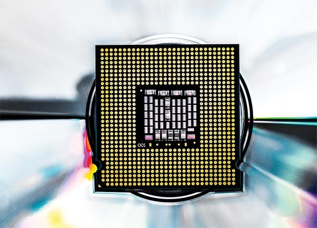
Courtesy of iStock.com/Mick Koulavong.
One area of notable advancement is in positioning technology and equipment: For structures in the nanometer-size range, it is critical to optimize positioning technology to meet the requirements of a given production process. As the physical capabilities of this technology have progressed, the emergence of intelligent solutions in nanopositioning technology have further established opportunities to achieve extremely high levels of precision.
As a result, advancements in positioning technology — paired with several key drivers from within industry — are enabling the creation of smaller, more powerful, and energy-efficient semiconductor devices.
Individual requirements
Industrial positioning systems for the semiconductor and electronics industry are typically configured individually to meet the distinctive requirements of an individual production task. Though different production processes may appear similar, or achieve similar outcomes, the need for individual configuration stems precisely from the stringent nature of these requirements.
Industrial positioning systems are characterized and evaluated based on several factors, ranging from accuracy and repeatability to physical, in-process requirements. For example, travel distances, or the required process area, is a crucial parameter and is used to indicate which distances the positioning system can cover in the axial directions. Similarly, step size, which refers to the smallest step or minimum incremental motion (MIM) that a device can reliably execute continuously, is a parameter that may be difficult to obtain. MIM values are commonly mistaken for resolution (R) values and may not be specified by all equipment manufacturers. In fact, step size, and MIM itself, does not correspond to the resolution of the encoder. This parameter may also be determined using methods that are not consistent from manufacturer to manufacturer.

To maintain high accuracy and repeatability
for positioning systems, manufacturers offer
calibration services to determine the error
topography of a mechanical platform. Courtesy of MKS Newport.
Additional factors that a user may conflate are repeatability and accuracy. Repeatability describes the ability of a system to reliably approach the same position several times in response to the same command. Within this parameter, there is a distinction between unidirectional and bidirectional repeatability. With bidirectional repeatability, approaching the position from both directions is considered, so that the reversal error when changing positions is also considered.
On the other hand, absolute accuracy quantifies the deviation between the actual and target positions. Accuracy can be specified in terms of total travel, or per-unit length.
Optimizing step-and-settle time, or the time that it takes to move from one measuring or processing point to the next, and to settle stably on it within a definable position window, is another crucial factor affecting performance and process results. The guidance deviation of an ideal linear motion, as indicated by straightness and flatness, presents yet another variable that a user must monitor. If a movement is carried out exclusively in the x direction, flatness refers to any deviation in the z
direction. Straightness, meanwhile, pertains to any deviation in the y direction.
Material Properties of Air Bearing Stage Materials

d: density measurement; E: Young’s modulus (stress/strain measurement of an elastic material, measured in gigapascals (GPa)). Courtesy of MKS Newport.
Depending on the application, mechanical and air-bearing positioning systems, also called air-bearing stages, may also be used. In classic positioning systems, the carriage slides over mechanical-ball or crossed-roller bearings. In air-bearing positioning systems, the carriage moves on a thin layer of clean compressed air or gas.
Finally, if only one of the axes requires very high precision, a hybrid system is a good option. These solutions use air bearings to position in only the one axis (the scanning axis), while positioning along the second is carried out mechanically (the stepping axis).
Positioning systems in-vacuum
The optimal positioning system for a given application depends on the required specifications as well as the available budget. However, the use of air-bearing systems has a fundamental limiting factor: They cannot be operated inside vacuum chambers. Because lithography processes used in/for semiconductor manufacturing that operate with extreme-ultraviolet light require an ultrahigh vacuum, mechanical bearings are the suitable component.
To achieve necessarily high accuracy and repeatability for this application, manufacturers such as MKS additionally offer the calibration of the mechanical positioning systems to determine the error topography of a mechanical platform. For a classic 300- × 300-mm wafer, for example, the grid is scanned in 10-mm steps, and an interferometer can be used to determine the exact position. This value is compared against the encoder value to determine the offset. The correction data set this comparison generates is stored in the motion controller and is used to improve the accuracy of the motion system.
This approach yields significantly higher absolute accuracy: For example, in tests to map an xy unit from two standard Newport XML350-S axes, the absolute accuracy improved by at least by a factor of 10. Since the axes are not perfectly orthogonal to each other in this instance, the combined error turns out to be much larger than just the sum of the two individual accuracies — it would certainly be significantly >10 µm in the 300- × 300-mm plane. But after mapping, the system achieved an absolute accuracy of <0.5 µm in the xy plane.
Air bearings: Frictionless precision
When inspecting wafers or masks for lithography applications that require maximum levels of precision, air-bearing positioning systems offer significant advantages. The load can be moved either linearly or rotationally, depending on the design of the system. And unlike traditional ball or crossed-roller bearings, there is no mechanical contact when moving an air-bearing stage.
Since there is neither play between the interacting mechanical parts of the drive system nor friction in the bearings, these elements can create several distinct advantages. First, it fundamentally eliminates the typical sources of error in mechanical bearings. And due to the planar structure with only one sliding carriage in the xy plane, the design is also significantly flatter than those with fully mechanical systems. This leads to considerably lower angular error(s) and better flatness and straightness value(s). At the same time, due to the lack of friction, air-bearing systems generate less heat, and positional stability is greater than in fully mechanical systems. Furthermore, the system can be moved at a consistent speed. The speed stability of air-bearing positioning systems is >0.1% — with step sizes down to just a few nanometers.

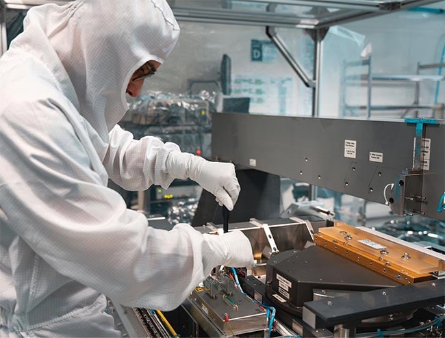
Semiconductor production requires
positioning systems that are finely tuned
and tailored to meet distinct and precise
requirements. Courtesy of iStock.com/kynny.
If the requirements in both absolute accuracy and travel speed values of a positioning system are high, positioning systems with a sliding carriage made of silicon carbide (SiC) offer significant benefits. This ceramic composite combines the positive properties of several individual materials, as shown in the table. It is as stiff as steel, as light as aluminum, and exhibits a thermal expansion coefficient similar to that of granite.
Due to the high rigidity of the slide and its low weight, such air-bearing systems work more dynamically, and therefore achieve a higher throughput than conventional systems. Plus, a SiC sliding carriage can offer additional flexibility in design. The overall high degree of integration with just a few individual components makes the positioning system more robust and increases its service life.
Intelligent solutions
Additional adjustments can influence the overall performance of a system to meet the unique requirements of an application. For example, the use of a SiC wafer chuck is recommended to achieve a high throughput rate in wafer production. Compared with a metal structure, this chuck is lighter and flatter and has the same thermal properties as the sliding carriage. This means that the components are optimally coordinated with each other. In addition, the wafer chuck can be integrated directly into the xy sliding carriage, if necessary, which ensures the low overall height of the setup. This enhances both the precision and the dynamics of the complete system.
For applications that require extreme levels of xy accuracy, interferometer-based solutions can be used in addition to classic displacement measurement systems, such as linear encoders. A mapping concept, such as the one described earlier, is integrated into the positioning system such that the position is read directly at the measuring point, eliminating, for example, encoder interpolation or Abbe error(s). Suppliers including MKS can integrate ceramic interferometer mirror solutions, which have excellent surface quality and dynamic properties, into positioning systems. As in the case of the wafer chuck, these ceramic mirrors can be built directly into the xy slide, so that they are an integral part of the positioning system and fit into the overall concept of the positioning platform in terms of their thermal properties.
Still other processes in lithography and/or wafer inspection may require active alignment of the wafer on the z-axis, in “tip and tilt,” or in the theta range. For this purpose, repeatable and stable positioning, without compromising the dynamic performance of the xy stage, is necessary.
Miniaturization: Underlying factors
Numerous drivers are combining to collectively push the semiconductor industry to continue developing smaller, more efficient, and more powerful technologies. These drivers exist despite the growing challenges associated with further scaling. In some cases, these drivers themselves have already spurred innovations in manufacturing processes and/or components and systems.
Certain advancements, such as those in lithography (particularly extreme-ultraviolet lithography) have allowed for more precise patterning at smaller scales, enabling the production of smaller features on chips. Moore’s law itself requires lithographic advancements; the number of transistors on a chip would double approximately every two years, leading to increased performance and reduced cost per transistor. This has led to continuous advancements in miniaturization to keep up with industry’s expectations, and the subsequent development of smaller, more densely packed transistors.
Material innovations in the form of new materials and processes have meanwhile enabled manufacturers to overcome the physical limitations of traditional silicon-based transistors. High-k/metal gate (HKMG) stacks, fin field-effect transistors (FinFETs), and gate-all-around (GAA) transistors all serve to meet this need. These materials allow for smaller and more efficient transistors, helping to maintain scaling even as traditional silicon-based approaches face physical limitations.
And since smaller transistors require less power and generate less heat, which is critical for the reliability and longevity of electronic devices, heat dissipation and power efficiency have emerged as core drivers to manufacturing at scale. This, paired with a growing need to integrate more functionality onto a single chip, has pushed miniaturization further into manufacturers’ focus. Miniaturization allows for more complex systems on-chip, which can integrate diverse functionalities into smaller form factors.
External factors are also causing a shift toward sustained miniaturization. Reductions in the cost per transistor are necessary for industry players to remain competitive, which has in turn created a need for smaller, more efficient manufacturing processes. Miniaturization allows for more transistors per wafer, reducing costs and improving yields, which is crucial for economic viability in producing advanced semiconductors. Also, consumer electronics, especially mobile devices, demand increasingly smaller, faster, and more energy-efficient components. The consumer market’s push for thinner, lighter, and more powerful devices is a major contributor to ongoing miniaturization in semiconductors.
Looking forward
Positioning systems used in semiconductor and consumer electronics production are finely tuned systems that are individually adapted to the respective requirements. Their configuration requires expertise and experience, and their manufacture is complex and subject to stringent specifications. For this reason, air-bearing stages, in particular, are only offered by several manufacturers worldwide. Close collaboration between the chip tool maker, or system integrator, and the positioning systems manufacturer in the design process is essential to ensure desired performance. Choosing the proper technologies and adapting them individually, though in combination with intelligent concepts, is necessary to guarantee the overall success of a project.
This is especially important to consider in the context of the anticipated manufacturing road map for the semiconductor and consumer electronics sectors. Tiny structure sizes of just a few nanometers have already been planned for the next generation of chips. And already the number of transistors on a given chip is constantly setting records. This level of integration can only be achieved if manufacturing technology keeps pace. Whether in the lithography itself, the inspection of wafers and masks, or in the bonding of different components, countless processing operations require positioning technology that is highly precise and reliable. Logically, the positioning accuracy must be even more fine-grained than the structures themselves.
Of course, these are not the only challenges. Reconciling the required precision and manufacturing quality of necessary process steps with the target throughput represents a dynamic on which all manufacturers must place a premium. Logistic decisions are also paramount. Automated systems, which are increasingly prevalent in wafer production and inspection, usually operate 24/7. Therefore, they place high demands on system availability.
Meet the authors
Knut Hauke is Newport senior sales territory manager at Newport Spectra-Physics GmbH, based in Darmstadt, Germany; email:
[email protected].
Marc Schenkelberger, Ph.D., is Newport sales manager for Newport Spectra-Physics GmbH; email:
[email protected].